


NCEPower NCE4963

- Part No.:
- NCE4963
- Manufacturer:
- NCEPower
- Category:
- P-Channel MOSFETs
- Package:
- Description:
- NCE4963 — 20V Dual P-Channel MOSFET (SOP-8)The NCE4963 is the logic-level end of this family — a dual P-channel 20V MOSFET in SOP-8, −7A per channel, 27mΩ max at −4.5V and 39mΩ max at −2.5V, from Wuxi NCE Power, da…
- Quantity:
-
Unit Price:$0
Ext Price:$0
- Payment:
-

- Shipping:
-


NCE4963 Information
- Specifications
- Product Details
- Comparison
- Tags
- Product attributes
- Attribute value
- Manufacturer:
- NCEPower
- Package/Case:
- Series:
- Packaging:
- SOP-8
- Product Status:
- Production
- FET Type:
- Industrial grade
- Technology:
- Trench双芯
- Drain to Source Voltage (Vdss):
- P+P
- Current - Continuous Drain (Id) @ 25°C:
- -20
- Drive Voltage (Max Rds On, Min Rds On):
- -7
- Rds On (Max) @ Id, Vgs:
- -0.7
- Vgs(th) (Max) @ Id:
- Gate Charge (Qg) (Max) @ Vgs:
- Vgs (Max):
- 19
- Input Capacitance (Ciss) (Max) @ Vds:
- 25
- FET Feature:
- 23
- Power Dissipation (Max):
- 32
- Operating Temperature:
- ±12
- Grade:
- 1210
- Qualification:
- 10
- Mounting Type:
- 3
- Supplier Device Package:
- 供应商设备封装:
- 供应商设备封装:
- 控制特性:
- 认证机构:
- 标准编号:
- Current Rating (Amps):
- param_30:
NCE4963 — 20V Dual P-Channel MOSFET (SOP-8)
The NCE4963 is the logic-level end of this family — a dual P-channel 20V MOSFET in SOP-8, −7A per channel, 27mΩ max at −4.5V and 39mΩ max at −2.5V, from Wuxi NCE Power, datasheet v2.0.
From what we see across Shenzhen lots (2025–2026), this part gets specified when the rail is a single lithium cell and the only gate voltage available is whatever the logic runs at.
It is the lowest-resistance member of the three-part dual shelf — 27mΩ against the NCE4953's 55mΩ — and it has the best thermal path, at 42°C/W. That is a real advantage.
But the trade is on the same page. Input capacitance is 1210pF against the NCE4953's 520pF, and turn-off delay is 70ns against 14ns. This is not a fast part.
And watch the gate window: VGS is ±12V here, not ±20V. The rail-voltage trap that costs the 30V siblings their margin arrives at half the voltage on this one.
What Are the Technical Specifications of NCE4963?
| Parameter | Value |
|---|---|
| Type | Dual P-Channel Enhancement Mode Power MOSFET (Trench) |
| Package | SOP-8, device marking “4963” |
| Drain-Source Voltage (VDS) | −20V |
| Gate-Source Voltage (VGS) | ±12V max |
| Continuous Drain Current (ID) | −7A per channel |
| Pulsed Drain Current (IDM) | −40A |
| RDS(on) @ −4.5V | 27mΩ max (typ 21mΩ, ID = −6.5A) |
| RDS(on) @ −2.5V | 39mΩ max (typ 29mΩ, ID = −5A) |
| Gate Threshold Voltage (VGS(th)) | −0.6V min / −0.8V typ / −1.4V max |
| Forward Transconductance (gfs) | 10S typ (VDS = −5V, ID = 3A) |
| Input Capacitance (Ciss) | 1210pF (VDS = −10V) |
| Output / Reverse Transfer Capacitance | 310pF / 290pF |
| Total Gate Charge (Qg) @ −4.5V | 10nC (Qgs 1.5nC, Qgd 3nC) |
| Switching Times (td(on)/tr/td(off)/tf) | 25 / 30 / 70 / 50 ns (VDD = −10V, ID = −1A, RGEN = 6Ω) |
| Drain-Source Breakdown (BVDSS) | −20V min (ID = −250µA) |
| Body Diode Forward Voltage (VSD) | −1.2V max (IS = −7A) |
| Max Power Dissipation (PD) | 3.0W — one package-level rating, not split per channel |
| Thermal Resistance (RθJA) | 42°C/W — the best of the three, still FR4 t ≤ 10 sec |
| Operating Junction & Storage Temperature | −55°C to 150°C |
| Reel / Tape | Ø330mm, 12mm tape, 2500 units |
Two rows deserve a second look. The threshold is −0.8V typical — genuinely low, and the reason this part can be driven from 2.5V logic at all. And the gate window is ±12V, half of what the 30V siblings allow.
Put together, that is a narrow band to design in. You need enough gate swing to reach the published resistance rows, and not so much that you approach the 12V limit.
Here is what those resistance rows cost at the headline current:
This is the easiest of the three parts to keep cool. Even at 2.5V drive and full rated current, one channel sits at 64% of a 3W budget — where the NCE4953 reaches 94% of its own 2.5W budget at a higher gate voltage.
But why does the low-resistance, low-threshold part switch so much more slowly? Because 1210pF of input capacitance has to be charged and discharged by a gate drive that is, by definition, low voltage. Low threshold and low gate swing buy conduction loss back at the cost of switching loss.
When Should You Use (and NOT Use) the NCE4963?
✅ Use NCE4963 when:
- Your rail is a single lithium cell or a 12V-and-under bus. The −20V rating fits these rails with margin, and using a 30V part here buys nothing.
- Your logic is 2.5V. This is the only part of the three characterized at 2.5V gate drive — 39mΩ max is a number you can design to, not a guess.
- Conduction loss dominates and switching is slow by design. Load switches, battery disconnect paths and static high-side gates are exactly where 27mΩ pays off without punishing the slow edges.
- Thermal headroom is tight. 42°C/W is the best thermal path in the family, and 3.0W of package budget is 20% more than the NCE4953 offers.
- Motor drive and load-switch duty at low frequency. Both applications are named on the sheet, and both tolerate 25–70ns edges.
❌ Don't use NCE4963 when:
- You are switching at any real frequency. 70ns turn-off delay and 1210pF of input capacitance make this a conduction-optimized part. Push the frequency and the switching loss will overtake what the low RDS(on) saved.
- Your gate drive swings above 12V, or your rail does. ±12V is half the window of the 30V siblings. A resistive pull-up from a 12V rail already sits at the limit — there is no margin left for ringing.
- You need more than 20V of blocking. This is a 20V part. Inductive rails that ring past 20V will take it out; the NCE4953 or NCE4606 covers 30V.
- You need a complementary pair. Both channels are P-channel. The NCE4606 is the part with one of each.
- Your load generates unclamped inductive edges. No EAS row and no body-diode trr row are published for this part either.
What Are the Alternatives to NCE4963?
| Model | Type | Key Difference | Best For |
|---|---|---|---|
| NCE4953 | Dual P-Channel 30V, SOP-8 | Higher voltage and a ±20V gate window, but 55mΩ at −10V and only characterized down to −4.5V — and its switching is 5× faster | 30V rails with a 10V or 4.5V gate drive |
| NCE4606 | Complementary N+P 30V, SOP-8 | One N-channel and one P-channel, for a level-shifted high-side switch — but its resistance rows are 10V-only | Circuits needing both polarities |
| NCE9926 | Dual N-Channel 20V, SOP-8 | Two N-channels at 20V/6A with a 2.5V-drive spec — the low-side equivalent of this part | Low-side switching from logic levels |
| NCE9435 | Single P-Channel 30V, SOP-8 | −30V/−5.1A in one channel — use it when you need one switch, not two | A single high-side switch |
Here is the honest trade in one line: you get the best resistance and the best thermal path in the family, and you pay for both with switching speed and gate-window margin. Whether that is a good deal depends entirely on how fast the channel has to move.
What about your switching frequency — is this a static switch or a PWM stage? If it holds a load on and off, the 27mΩ is free money. If it chops at tens of kHz, the NCE4953's 14ns edges will beat it despite the higher resistance.
The pin map is identical to the NCE4953: S1 on pin 1, G1 on pin 2, S2 on pin 3, G2 on pin 4, with D1 on pins 7 and 8 and D2 on pins 5 and 6. The pin-1 dot is at the lower left on both parts.
That is convenient between these two — and dangerous against the NCE4606. The complementary part puts S2/G2 on pins 1 and 2 and S1/G1 on pins 3 and 4: same package, swapped channel numbers.
Both drive levels clear the budget well past normal ambient — one channel at 2.5V drive crosses the derating line around 70°C, and at 4.5V drive at 95°C. That is the payoff for the 42°C/W thermal path, derived from the datasheet rows rather than a published curve.
One detail worth knowing if you rebuild this chart: the sheet prints 3.0W and 42°C/W together, and they disagree slightly — (150−25)/42 comes to 2.98W. The line here follows the printed 3.0W figure, which is the one the table quotes.
What Are the Typical Applications of NCE4963?
Motor drive at low voltage. The sheet names it first, and the combination of −20V, −7A and 27mΩ fits small brushed motors and actuator loads driven from a single cell or a low-voltage bus.
Load switches on battery rails. This is where the low threshold earns its keep: a 2.5V logic output can enhance the channel, and 39mΩ max at that drive is a real number rather than an extrapolation.
Battery disconnect and protection paths. The body diode carries the reverse path, and two independent channels let you switch the pack and a secondary rail separately.
Static high-side gates where switching loss is irrelevant. If the channel holds a load on for seconds or minutes, the 1210pF and 70ns edges cost nothing — and the low RDS(on) is pure gain.
Why Buy NCE4963 from ICMASS?
We sample-test NCE4963 lots at both logic-level conditions: 27mΩ max at −4.5V and 39mΩ max at −2.5V. A part sold on logic-level drive has to be verified at logic level, not at 10V.
The clone market reaches this part too. VBsemi's NCE4963-VB is a separately-branded dual P-channel 20V SOP-8 with its own datasheet and different ratings — a −8.9A claim and a 16mΩ figure at 10V, a drive level this part is not characterized at. Genuine parts are marked “4963” and match this sheet.
The whole dual shelf is stocked together: NCE4963 and NCE4953 for two P-channels, the complementary NCE4606, and the dual-N NCE9926, each with its official PDF on hand. When the honest answer is the faster 30V part, we will say so.
Orders ship same day from Shenzhen, with volume pricing that keeps a genuine 20V logic-level dual-P SOP-8 competitive against clone stock wearing a similar code.
Frequently Asked Questions About NCE4963
Q1: Can I really drive the NCE4963 from 2.5V logic?
A: Yes — it is characterized there, which is rare. The threshold is −0.8V typical (−1.4V max) and the sheet publishes a full RDS(on) row at −2.5V: 39mΩ max at −5A. Most parts in this class stop at 4.5V and leave you extrapolating. The 30V siblings in this family stop there too.
Q2: Why is VGS only ±12V when the other parts are ±20V?
A: It's the price of the low threshold. A thinner gate oxide enhances the channel at lower voltage, and it also breaks down at lower voltage. Practically: you don't want to hang this gate on a 12V rail through a resistor — that's exactly at the limit with no margin for ringing.
Q3: What is the catch compared to the NCE4953?
A: Switching speed. You gain resistance (27mΩ versus 55mΩ) and thermal headroom (42°C/W versus 50°C/W), but input capacitance goes from 520pF to 1210pF and turn-off delay from 14ns to 70ns. Below a few kHz this is free money; at tens of kHz it is a loss.
Q4: Is the pin map the same as the NCE4953?
A: Yes, identical. Pin 1 is S1, pin 2 is G1, pin 3 is S2, pin 4 is G2; D1 sits on pins 7 and 8 and D2 on pins 5 and 6. That makes these two drop-in alternatives for each other on the pin side — but not for the complementary NCE4606, whose channel numbers are swapped.
Q5: How much current can one channel carry continuously?
A: Better than its siblings, but still board-limited. At −7A one channel burns 1.32W at 4.5V drive and 1.91W at 2.5V drive, against a 3.0W package budget qualified at t ≤ 10 sec on FR4. That is 44% and 64% respectively — comfortable on paper, but the budget is shared if both channels run.
Q6: Is the 3.0W rating for one channel or both?
A: The sheet gives a single rating, so treat it as package-level. One RθJA row (42°C/W) and one PD row (3.0W). Two conducting channels share that budget — which still leaves more headroom than either 30V sibling provides.
Q7: Can it switch an inductive load without a clamp?
A: Not on the datasheet's authority. There is no EAS row and no body-diode trr row, so avalanche energy and commutation behaviour are unquantified. Motor and solenoid loads need a clamp or a snubber — the sheet names motor drive as an application, but it does not publish an avalanche budget for it.
Q8: How do I tell a genuine NCE4963 from the clone?
A: Marking plus the datasheet's own ratings. Genuine parts are marked “4963”, are −20V/−7A with a ±12V gate window, and publish 27mΩ at −4.5V and 39mΩ at −2.5V. VBsemi's NCE4963-VB quotes a 16mΩ figure at 10V — a drive level the NCE original does not characterize at all.
| Image |

|
| Part Number | NCE4963 |
| Manufacturer | NCEPower |
| Package/Case | |
| Series | |
| Packaging | SOP-8 |
| Product Status | Production |
| FET Type | Industrial grade |
| Technology | Trench双芯 |
| Drain to Source Voltage (Vdss) | P+P |
| Current - Continuous Drain (Id) @ 25°C | -20 |
| Drive Voltage (Max Rds On, Min Rds On) | -7 |
| Rds On (Max) @ Id, Vgs | -0.7 |
| Vgs(th) (Max) @ Id | |
| Gate Charge (Qg) (Max) @ Vgs | |
| Vgs (Max) | 19 |
| Input Capacitance (Ciss) (Max) @ Vds | 25 |
| FET Feature | 23 |
| Power Dissipation (Max) | 32 |
| Operating Temperature | ±12 |
| Grade | 1210 |
| Qualification | 10 |
| Mounting Type | 3 |
| Supplier Device Package | |
| 供应商设备封装 | |
| 供应商设备封装 | |
| 控制特性 | |
| 认证机构 | |
| 标准编号 | |
| Current Rating (Amps) | |
| param_30 |
User Guide
- Purchase & Inquiry
- Package
- Shipping Information
- Customer Review
You may place an order without registering to IC-MAX.COM
We strongly suggest you sign in before purchasing as you can track your order in real time.
For your convenience, we accept multiple payment methods in USD, including PayPal, Credit Card, and wire transfer.
RFQ (Request for Quotations)
It is recommended to request for quotations to get the latest prices and inventories about the part.
Our sales will reply to your request by email within 24 hours.
1. You'll receive an order information email in your inbox. (Please remember to check the spam folder if you didn't hear from us).
2. Since inventories and prices may fluctuate to some extent, the sales manager is going to reconfirm the order and let you know if there are any updates.
-
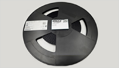
- Step1:Prepare product
-
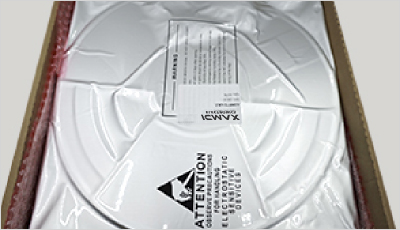
- Step2:Vacuum packaging
-
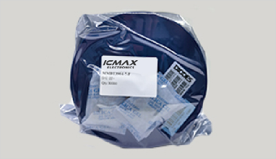
- Step3:Anti-static bag
-
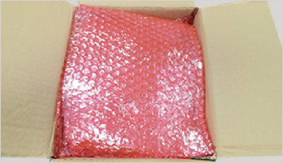
- Step4:Individual package
-
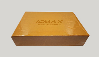
- Step5:Packaging box
-
- Step6:Barcode shipping label
Shipping starts at $40, but some countries will exceed $40. For example (South Africa, Brazil, India, Pakistan, Israel, etc.)
The basic freight (for package ≤0.5kg or corresponding volume) depends on the time zone and country.
Currently, our products are shipped through DHL, FedEx, SF, and UPS.
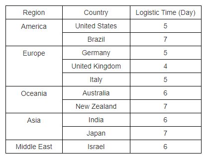
Delivery TimeOnce the goods are shipped, estimated delivery time depends on the shipping methods you chose:
FedEx International, 5-7 business days.
The following are some common countries' logistic time.
- Hot Sale
- Related Categories
- Include Parts
- Popular Search
The following parts include "NCE4963" in Silicon Labs NCE4963.
- Part Number
- Manufacturer
- Package
- Description
- NCE2305A NCEPower NCE4963 — 20V Dual P-Channel MOSFET (SOP-8)The NCE4963 is the logic-level end of this family — a dual P-channel 20V MOSFET in SOP-8, −7A per channel, 27mΩ max at −4.5V and 39mΩ max at −2.5V, from Wuxi NCE Power, da…
- NCE2305 NCEPower NCE4963 — 20V Dual P-Channel MOSFET (SOP-8)The NCE4963 is the logic-level end of this family — a dual P-channel 20V MOSFET in SOP-8, −7A per channel, 27mΩ max at −4.5V and 39mΩ max at −2.5V, from Wuxi NCE Power, da…
- NCE3401 : P-Channel 30V -4.2A Power MOSFET SOT-23 NCEPower NCE4963 — 20V Dual P-Channel MOSFET (SOP-8)The NCE4963 is the logic-level end of this family — a dual P-channel 20V MOSFET in SOP-8, −7A per channel, 27mΩ max at −4.5V and 39mΩ max at −2.5V, from Wuxi NCE Power, da…
- NCE9435 NCEPower NCE4963 — 20V Dual P-Channel MOSFET (SOP-8)The NCE4963 is the logic-level end of this family — a dual P-channel 20V MOSFET in SOP-8, −7A per channel, 27mΩ max at −4.5V and 39mΩ max at −2.5V, from Wuxi NCE Power, da…
- NCE30P12S NCEPower NCE4963 — 20V Dual P-Channel MOSFET (SOP-8)The NCE4963 is the logic-level end of this family — a dual P-channel 20V MOSFET in SOP-8, −7A per channel, 27mΩ max at −4.5V and 39mΩ max at −2.5V, from Wuxi NCE Power, da…
- NCE30P25S NCEPower NCE4963 — 20V Dual P-Channel MOSFET (SOP-8)The NCE4963 is the logic-level end of this family — a dual P-channel 20V MOSFET in SOP-8, −7A per channel, 27mΩ max at −4.5V and 39mΩ max at −2.5V, from Wuxi NCE Power, da…
- NCE30P30K NCEPower NCE4963 — 20V Dual P-Channel MOSFET (SOP-8)The NCE4963 is the logic-level end of this family — a dual P-channel 20V MOSFET in SOP-8, −7A per channel, 27mΩ max at −4.5V and 39mΩ max at −2.5V, from Wuxi NCE Power, da…
- NCE30P30G NCEPower NCE4963 — 20V Dual P-Channel MOSFET (SOP-8)The NCE4963 is the logic-level end of this family — a dual P-channel 20V MOSFET in SOP-8, −7A per channel, 27mΩ max at −4.5V and 39mΩ max at −2.5V, from Wuxi NCE Power, da…
- NCE30P50G NCEPower NCE4963 — 20V Dual P-Channel MOSFET (SOP-8)The NCE4963 is the logic-level end of this family — a dual P-channel 20V MOSFET in SOP-8, −7A per channel, 27mΩ max at −4.5V and 39mΩ max at −2.5V, from Wuxi NCE Power, da…
- NCE2309 — P-Channel 60V/1.6A Enhancement Mode Power MOSFET (SOT-23) NCEPower NCE4963 — 20V Dual P-Channel MOSFET (SOP-8)The NCE4963 is the logic-level end of this family — a dual P-channel 20V MOSFET in SOP-8, −7A per channel, 27mΩ max at −4.5V and 39mΩ max at −2.5V, from Wuxi NCE Power, da…
The following parts are popular search parts in Test and Measurement.
Inventory:50,000
Please send an inquiry. Send us your inquiry, and we will respond immediately.

- 1500+ Daily average RFQ Volume

- 20,000.000 Standard Product Unit

- 1800+ Worldwide Manufacturers

- 15,000+ In-stock Warehouse


