


NCEPower NCE2309 — P-Channel 60V/1.6A Enhancement Mode Power MOSFET (SOT-23)

- Part No.:
- NCE2309 — P-Channel 60V/1.6A Enhancement Mode Power MOSFET (SOT-23)
- Manufacturer:
- NCEPower
- Category:
- P-Channel MOSFETs
- Package:
- Description:
- NCE2309 – NCE Power P-Channel Enhancement Mode Power MOSFETQuick Answer The NCE2309 is a P-Channel Enhancement Mode Power MOSFET from Wuxi NCE Power Semiconductor.
- Quantity:
-
Unit Price:$0
Ext Price:$0
- Payment:
-

- Shipping:
-


NCE2309 — P-Channel 60V/1.6A Enhancement Mode Power MOSFET (SOT-23) Information
- Specifications
- Product Details
- Comparison
- Tags
- Product attributes
- Attribute value
- Manufacturer:
- NCEPower
- Package/Case:
- Series:
- Packaging:
- SOT-23
- Product Status:
- Production
- FET Type:
- Industrial grade
- Technology:
- Trench
- Drain to Source Voltage (Vdss):
- P
- Current - Continuous Drain (Id) @ 25°C:
- -60
- Drive Voltage (Max Rds On, Min Rds On):
- -1.6
- Rds On (Max) @ Id, Vgs:
- -2
- Vgs(th) (Max) @ Id:
- 140
- Gate Charge (Qg) (Max) @ Vgs:
- 160
- Vgs (Max):
- 160
- Input Capacitance (Ciss) (Max) @ Vds:
- 200
- FET Feature:
- Power Dissipation (Max):
- Operating Temperature:
- ±20
- Grade:
- 444.2
- Qualification:
- 11
- Mounting Type:
- 1.5
- Supplier Device Package:
- 供应商设备封装:
- 供应商设备封装:
- 控制特性:
- 认证机构:
- 标准编号:
- Current Rating (Amps):
- param_30:
NCE2309 - P-Channel 60V/1.6A Enhancement Mode Power MOSFET (SOT-23)
The NCE2309 is a P-channel enhancement mode power MOSFET from Wuxi NCE Power, rated at -60V drain-source with -1.6A continuous drain current in a SOT-23 package.
If you need a high-side load switch on a 12V, 24V, or 48V rail without a gate driver IC, this is the part. The ±20V VGS rating gives headroom the NCE3400 (±12V) lacks. In a 24V system, you pull gate-to-ground with no oxide stress.
The 190mΩ RDS(on) at -10V VGS keeps conduction losses under half a watt at full load. And the "2309" marking is an industry standard - SI2309, ME2309, SL2309 share the same footprint. You're never single-sourced on this part.
What Are the Technical Specifications of NCE2309?
| Parameter | Value |
|---|---|
| Type | P-Channel Enhancement Mode Power MOSFET |
| Package | SOT-23-3L (surface mount) |
| Drain-Source Voltage (VDSS) | -60V |
| Gate-Source Voltage (VGSS) | ±20V |
| Continuous Drain Current (ID) | -1.6A @ 25°C |
| Pulsed Drain Current (IDM) | -8A (10µs pulse) |
| Power Dissipation (PD) | 1.5W @ 25°C |
| Gate Threshold Voltage (VGS(th)) | -1.4V min / -2.0V typ / -2.6V max @ -250µA |
| On-Resistance (RDS(on)) | 190mΩ max @ VGS=-10V, ID=-1.6A |
| On-Resistance (RDS(on)) | 200mΩ max @ VGS=-4.5V, ID=-1.6A |
| Total Gate Charge (QG) | ~11.3nC @ VDS=-30V, VGS=-10V |
| Input Capacitance (CISS) | ~444pF @ VDS=-30V |
| Output Capacitance (COSS) | ~20pF @ VDS=-30V |
| Operating Temperature | -55°C to +150°C |
| Thermal Resistance (RθJA) | 83.3°C/W (FR4 board, t≤10s) |
| Manufacturer | Wuxi NCE Power Semiconductor |
RDS(on) at each gate drive level. At -10V you get the full 190mΩ. At -4.5V it's only slightly higher at 200mΩ. The difference is marginal.
This matters in practice: if your MCU GPIO drives an NPN that pulls the gate to ground, you're working with -3.3V or -5V VGS. The RDS(on) is still well within spec at those levels.
Bar width = max RDS(on) relative to 200mΩ. The gap between typical and max is ~30mΩ at both gate levels - budget for worst case if your load is near the 1.6A limit.
SOT-23 pinout - P-channel, source to the high-side rail. Pin 1 is Gate (pull low to turn on). Pin 2 is Source (connect to supply). Pin 3 is Drain (connect to load).
This is the opposite convention from N-channel where Drain is the high side. If you're used to wiring N-channel parts, double-check the pinout before you send the layout out.
How the NCE2309 stacks up against common alternatives on RDS(on). The NCE60P04Y cuts resistance by over a third, but costs more. The AO6385 is the lowest-RDS(on) option in this voltage class. The SI2309 and SL2309 are functionally identical - pick whichever is in stock.
Bar width = RDS(on) max relative to NCE2309 (190mΩ). Lower RDS(on) means lower conduction loss, but the die size and cost go up. For a 1A load switch, the NCE2309's 190mΩ is fine - you're burning ~0.2W in the MOSFET.
When Should You Use (and NOT Use) the NCE2309?
✓ Use the NCE2309 when:
- You need a high-side load switch on a 12V–48V rail. P-channel parts turn on by pulling the gate low. No charge pump, no bootstrap capacitor, no gate driver IC. One NPN transistor and a pull-up resistor and you're done.
- Your gate drive is limited to 5V or 3.3V logic. At VGS=-4.5V the RDS(on) is only 10mΩ worse than at -10V. Compare that to N-channel high-side switches that need a gate voltage above the supply rail.
- You want second-source security on a commodity part. The "2309" footprint is shared across NCE, Vishay (SI2309), LRC (LP2309), Matsuki (ME2309), and others. If one brand goes on allocation, you swap in another without touching the PCB.
- You're doing battery reverse-polarity protection. P-channel in series with the positive rail, gate to ground, body diode blocks reverse current. The 60V rating covers 12V and 24V battery systems with margin.
✗ Don't use the NCE2309 when:
- Your load pulls more than 1.5A continuous. At 1.6A you're at the absolute maximum. Derate to 1A for margin, or step up to a higher-current P-channel part.
- You need sub-100mΩ RDS(on). This is a 190mΩ part. If your load is 2A and you can't afford 0.4W of conduction loss, look at NCE60P04Y (120mΩ) or AO6385 (85mΩ).
- Your switching frequency is above 200kHz. With ~11nC gate charge and 444pF input capacitance, switching losses start to dominate above a few hundred kHz. This part is optimised for load switching and low-frequency PWM, not high-speed DC-DC.
- You're driving an inductive load without a flyback diode. The body diode's reverse recovery time is ~25ns - fast, but it won't save you from inductive kickback. Always add a freewheeling diode across solenoids, motors, or relays.
What Are the Alternatives to NCE2309?
| Model | Manufacturer | Key Difference | Best For |
|---|---|---|---|
| SI2309CDS-T1-GE3 | Vishay | Lower RDS(on) (~50mΩ typ) | Higher-current designs, Western supply chain |
| NCE60P04Y | NCE Power | 120mΩ RDS(on), higher ID | Lower conduction loss in same SOT-23 footprint |
| AO6385 | Alpha & Omega | 85mΩ RDS(on), 3A ID | Lowest RDS(on) in 60V P-Ch SOT-23 class |
| SL2309 | Secland | Near-identical specs (165mΩ typ) | Direct swap, often lower cost in Asia |
| NCEA2309 | NCE Power | Same die, AEC-Q101 qualified | Automotive and harsh-environment applications |
| ME2309 | Matsuki | 215mΩ, slightly wider VGS(th) | Budget alternative, high-volume consumer |
The "2309" ecosystem is deep. Eight manufacturers make a pin-compatible 60V P-Ch SOT-23 with this marking. If you're cost-sensitive, SL2309 and ME2309 are typically the cheapest. If you need reliability data, the NCEA2309 gives you AEC-Q101 qualification with the same electrical specs.
What Are the Typical Applications of NCE2309?
High-side load switching. This is what the part was designed for. Source to the supply rail, drain to the load, gate pulled low by an NPN or open-drain GPIO to turn on. No charge pump needed - that's the entire point of using a P-channel MOSFET for high-side switching.
Battery reverse-polarity protection. Place the NCE2309 in series with the positive battery terminal, source to battery, drain to circuit, gate to ground. If someone inserts the battery backwards, VGS is positive and the MOSFET stays off. At 190mΩ you lose ~0.3V at 1.6A - acceptable for most battery-powered designs.
Overvoltage cutoff for 48V telecom and PoE. The 60V VDSS rating gives enough headroom for 48V nominal rails (which can spike to 54V). Use a Zener + resistor divider on the gate to clamp the turn-on threshold. When the rail exceeds the Zener voltage, the MOSFET shuts off.
USB PD power path control. At 20V USB PD, the NCE2309's 60V rating is overkill, but the low gate charge means fast turn-on when a power source is detected. Useful for OR-ing two power inputs: one NCE2309 per input, gates controlled by a comparator.
LED lighting and small motor PWM. At low PWM frequencies (a few kHz), the NCE2309 switches cleanly. The 11nC gate charge means a 10mA GPIO can drive it directly through a base resistor on the NPN driver. Keep PWM below 10kHz and switching losses are negligible.
High-Side Switching with NCE2309: The Circuit That Trips People Up
P-channel high-side switches are simple on paper. Source to V+, drain to load, pull gate low to turn on. Three pins, no charge pump. So why do boards come back with the load permanently powered?
The body diode orientation trap. For P-channel, the body diode anode is on the drain side, cathode on the source. Current flows drain→source through the diode even with VGS=0.
If you swap source and drain, the load is always on. No amount of gate voltage turns it off - the body diode conducts regardless.
The fix: source to supply rail, drain to load. In a SOT-23 where pin 2 is Source and pin 3 is Drain, this mistake is surprisingly common on first layouts.
Gate pull-up resistor sizing. A 100kΩ pull-up from gate to source keeps the MOSFET off by default. But with 444pF input capacitance, the RC time constant is ~44µs. If your circuit switches rapidly, every transition spends 44µs in the linear region generating heat.
Drop the pull-up to 10kΩ and turn-off shrinks to ~4.4µs. The trade-off: 10kΩ at 24V burns 2.4mA quiescent. For battery-powered devices, keep the 100kΩ. For mains-powered designs, use 10kΩ.
VGS clamping for 48V rails. The NCE2309 has a ±20V VGS rating. In a 48V system, pulling the gate to ground puts 48V across gate-source. That's instant oxide failure.
The fix: a 15V Zener between gate and source. Without it, the MOSFET works for a few cycles then fails short. With it, the circuit runs for years.
Why Buy NCE2309 from ICMASS?
We stock the full 2309 family. NCE2309, SI2309, SL2309, and the automotive-grade NCEA2309. If your BOM calls for a 60V P-Ch SOT-23, we have an approved second-source ready to ship.
Gate threshold testing available on request. VGS(th) varies across production batches. If your design depends on the MOSFET turning fully on at a specific gate voltage, we can verify threshold distribution on your lot before it leaves Shenzhen.
Cross-reference support for the 2309 ecosystem. Need to swap from SI2309 to NCE2309? Or from NCE2309 to a lower-RDS(on) upgrade like NCE60P04Y? We'll confirm pinout, gate drive compatibility, and any layout changes needed.
Frequently Asked Questions
Q1: What's the difference between NCE2309 and NCE3400?
A: NCE2309 is P-channel (-60V), NCE3400 is N-channel (30V). They are complementary parts for different switching topologies. Use NCE2309 for high-side switching (source to V+), NCE3400 for low-side switching (source to GND). The NCE2309 also has a wider VGS rating (±20V vs ±12V).
Q2: Can I use NCE2309 to replace an SI2309?
A: Yes, drop-in replacement. Same SOT-23 pinout, same 60V rating. The NCE2309 has slightly lower RDS(on) (190mΩ vs 215mΩ), so it runs marginally cooler. No firmware or layout changes needed.
Q3: Why does my P-channel high-side switch stay on even when the gate is pulled high?
A: Check if source and drain are swapped. The body diode conducts drain-to-source even with VGS=0. Source must go to the supply rail, drain to the load. Also check your gate pull-up resistor - if it's open-circuit or too high, leakage current on the gate node can partially enhance the MOSFET.
Q4: Do I need a gate resistor for NCE2309?
A: For load switching, a small series gate resistor (100Ω–1kΩ) is good practice. It suppresses parasitic oscillation during switching. For PWM above a few kHz, keep it low (100Ω) to avoid slowing down the gate too much. For pure DC on/off switching, the resistor value isn't critical.
Q5: What's the NCEA2309 variant?
A: Same silicon, AEC-Q101 automotive qualified. Same electrical specs as NCE2309, but each production lot goes through additional reliability testing (temperature cycling, HTRB, HAST). Use it if your design needs to meet automotive or industrial reliability standards.
Q6: Can NCE2309 handle 48V systems?
A: Yes, for the drain-source voltage. 60V VDSS covers 48V nominal with margin for transients. But protect the gate: a 48V rail will destroy the gate oxide (±20V max) unless you add a 15V Zener clamp between gate and source. This is not optional at 48V.
Q7: How does NCE2309 compare to using an N-channel MOSFET for high-side switching?
A: Simpler gate drive, but higher RDS(on). P-channel turns on by pulling gate low - no charge pump or bootstrap needed. The trade-off: P-channel parts have roughly 2–3× the RDS(on) of an equivalent N-channel at the same die size. For a 1A load switch, the simplicity usually wins. For 10A, you'd go N-channel with a gate driver.
Q8: What's the maximum PWM frequency I can run with NCE2309?
A: Practical limit is around 50–100kHz. At 11nC gate charge and 444pF input capacitance, switching losses become significant above 100kHz. For DC-DC converters running at hundreds of kHz, use a part with lower gate charge. For load switching and low-frequency PWM (motor control, LED dimming), it's fine.
| Image |

|
| Part Number | NCE2309 — P-Channel 60V/1.6A Enhancement Mode Power MOSFET (SOT-23) |
| Manufacturer | NCEPower |
| Package/Case | |
| Series | |
| Packaging | SOT-23 |
| Product Status | Production |
| FET Type | Industrial grade |
| Technology | Trench |
| Drain to Source Voltage (Vdss) | P |
| Current - Continuous Drain (Id) @ 25°C | -60 |
| Drive Voltage (Max Rds On, Min Rds On) | -1.6 |
| Rds On (Max) @ Id, Vgs | -2 |
| Vgs(th) (Max) @ Id | 140 |
| Gate Charge (Qg) (Max) @ Vgs | 160 |
| Vgs (Max) | 160 |
| Input Capacitance (Ciss) (Max) @ Vds | 200 |
| FET Feature | |
| Power Dissipation (Max) | |
| Operating Temperature | ±20 |
| Grade | 444.2 |
| Qualification | 11 |
| Mounting Type | 1.5 |
| Supplier Device Package | |
| 供应商设备封装 | |
| 供应商设备封装 | |
| 控制特性 | |
| 认证机构 | |
| 标准编号 | |
| Current Rating (Amps) | |
| param_30 |
User Guide
- Purchase & Inquiry
- Package
- Shipping Information
- Customer Review
You may place an order without registering to IC-MAX.COM
We strongly suggest you sign in before purchasing as you can track your order in real time.
For your convenience, we accept multiple payment methods in USD, including PayPal, Credit Card, and wire transfer.
RFQ (Request for Quotations)
It is recommended to request for quotations to get the latest prices and inventories about the part.
Our sales will reply to your request by email within 24 hours.
1. You'll receive an order information email in your inbox. (Please remember to check the spam folder if you didn't hear from us).
2. Since inventories and prices may fluctuate to some extent, the sales manager is going to reconfirm the order and let you know if there are any updates.
-
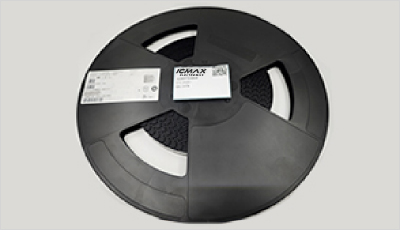
- Step1:Prepare product
-
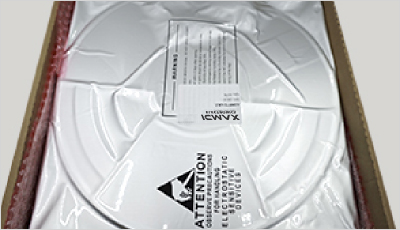
- Step2:Vacuum packaging
-
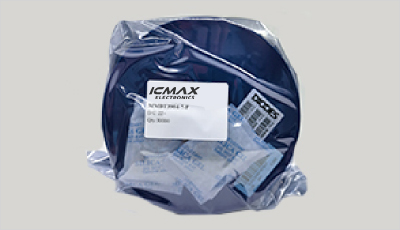
- Step3:Anti-static bag
-
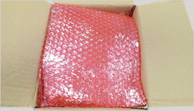
- Step4:Individual package
-
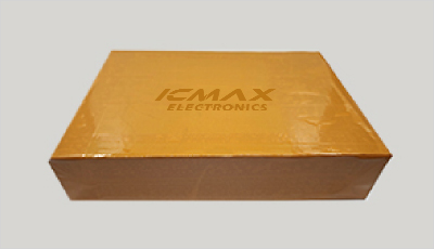
- Step5:Packaging box
-
- Step6:Barcode shipping label
Shipping starts at $40, but some countries will exceed $40. For example (South Africa, Brazil, India, Pakistan, Israel, etc.)
The basic freight (for package ≤0.5kg or corresponding volume) depends on the time zone and country.
Currently, our products are shipped through DHL, FedEx, SF, and UPS.
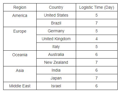
Delivery TimeOnce the goods are shipped, estimated delivery time depends on the shipping methods you chose:
FedEx International, 5-7 business days.
The following are some common countries' logistic time.
- Hot Sale
- Related Categories
- Include Parts
- Popular Search
The following parts include "NCE2309 — P-Channel 60V/1.6A Enhancement Mode Power MOSFET (SOT-23)" in Silicon Labs NCE2309 — P-Channel 60V/1.6A Enhancement Mode Power MOSFET (SOT-23).
- Part Number
- Manufacturer
- Package
- Description
- NCE2305A NCEPower NCE2309 – NCE Power P-Channel Enhancement Mode Power MOSFETQuick Answer The NCE2309 is a P-Channel Enhancement Mode Power MOSFET from Wuxi NCE Power Semiconductor.
- NCE2305 NCEPower NCE2309 – NCE Power P-Channel Enhancement Mode Power MOSFETQuick Answer The NCE2309 is a P-Channel Enhancement Mode Power MOSFET from Wuxi NCE Power Semiconductor.
- NCE3401 : P-Channel 30V -4.2A Power MOSFET SOT-23 NCEPower NCE2309 – NCE Power P-Channel Enhancement Mode Power MOSFETQuick Answer The NCE2309 is a P-Channel Enhancement Mode Power MOSFET from Wuxi NCE Power Semiconductor.
- NCE9435 NCEPower NCE2309 – NCE Power P-Channel Enhancement Mode Power MOSFETQuick Answer The NCE2309 is a P-Channel Enhancement Mode Power MOSFET from Wuxi NCE Power Semiconductor.
- NCE30P12S NCEPower NCE2309 – NCE Power P-Channel Enhancement Mode Power MOSFETQuick Answer The NCE2309 is a P-Channel Enhancement Mode Power MOSFET from Wuxi NCE Power Semiconductor.
- NCE30P25S NCEPower NCE2309 – NCE Power P-Channel Enhancement Mode Power MOSFETQuick Answer The NCE2309 is a P-Channel Enhancement Mode Power MOSFET from Wuxi NCE Power Semiconductor.
- NCE30P30K NCEPower NCE2309 – NCE Power P-Channel Enhancement Mode Power MOSFETQuick Answer The NCE2309 is a P-Channel Enhancement Mode Power MOSFET from Wuxi NCE Power Semiconductor.
- NCE30P30G NCEPower NCE2309 – NCE Power P-Channel Enhancement Mode Power MOSFETQuick Answer The NCE2309 is a P-Channel Enhancement Mode Power MOSFET from Wuxi NCE Power Semiconductor.
- NCE30P50G NCEPower NCE2309 – NCE Power P-Channel Enhancement Mode Power MOSFETQuick Answer The NCE2309 is a P-Channel Enhancement Mode Power MOSFET from Wuxi NCE Power Semiconductor.
- NCE2309 — P-Channel 60V/1.6A Enhancement Mode Power MOSFET (SOT-23) NCEPower NCE2309 – NCE Power P-Channel Enhancement Mode Power MOSFETQuick Answer The NCE2309 is a P-Channel Enhancement Mode Power MOSFET from Wuxi NCE Power Semiconductor.
The following parts are popular search parts in Test and Measurement.
Inventory:50,000
Please send an inquiry. Send us your inquiry, and we will respond immediately.

- 1500+ Daily average RFQ Volume

- 20,000.000 Standard Product Unit

- 1800+ Worldwide Manufacturers

- 15,000+ In-stock Warehouse


