


NCEPower NCE30P30K

- Part No.:
- NCE30P30K
- Manufacturer:
- NCEPower
- Category:
- P-Channel MOSFETs
- Package:
- Description:
- NCE30P30K — 30V/30A P-Channel Power MOSFET (TO-252-2L)The NCE30P30K is a -30V/-30A P-Channel trench MOSFET in TO-252-2L (DPAK) — 18mΩ max at 10V (typ 13mΩ), 31.2nC gate charge, and a spec sheet that answers the questions the sibling…
- Quantity:
-
Unit Price:$0
Ext Price:$0
- Payment:
-

- Shipping:
-


NCE30P30K Information
- Specifications
- Product Details
- Comparison
- Tags
- Product attributes
- Attribute value
- Manufacturer:
- NCEPower
- Package/Case:
- Series:
- Packaging:
- TO-252
- Product Status:
- Production
- FET Type:
- Industrial grade
- Technology:
- Trench
- Drain to Source Voltage (Vdss):
- P
- Current - Continuous Drain (Id) @ 25°C:
- -30
- Drive Voltage (Max Rds On, Min Rds On):
- -30
- Rds On (Max) @ Id, Vgs:
- -1.5
- Vgs(th) (Max) @ Id:
- 13
- Gate Charge (Qg) (Max) @ Vgs:
- 18
- Vgs (Max):
- 22
- Input Capacitance (Ciss) (Max) @ Vds:
- 30
- FET Feature:
- Power Dissipation (Max):
- Operating Temperature:
- ±20
- Grade:
- 1363
- Qualification:
- 31
- Mounting Type:
- 35
- Supplier Device Package:
- 供应商设备封装:
- 供应商设备封装:
- 控制特性:
- 认证机构:
- 标准编号:
- Current Rating (Amps):
- param_30:
NCE30P30K — 30V/30A P-Channel Power MOSFET (TO-252-2L)
The NCE30P30K is a -30V/-30A P-Channel trench MOSFET in TO-252-2L (DPAK) — 18mΩ max at 10V (typ 13mΩ), 31.2nC gate charge, and a spec sheet that answers the questions the sibling die leaves blank. From Wuxi NCE Power, datasheet v1.0.
From what we see across Shenzhen lots (2025–2026), this TO-252 die gets picked by two kinds of boards: designs already running the N-ch TO-252 line (same tab footprint, same assembly), and 10V-gate legacy systems where an 81nC charge is a driver problem waiting to happen.
The spec that doesn't get quoted enough: the K publishes what the DFN sibling does not — EAS 169mJ with conditions, ID -21.2A at 100°C, trr 24ns — at the price of 1.8× the on-resistance.
Buy the 30P30K for a light gate, a published avalanche budget, and a tab you can solder by hand — and respect the math: 30A through 18mΩ is 16.2W before anything else.
What Are the Technical Specifications of NCE30P30K?
| Parameter | Value |
|---|---|
| Type | P-Channel Enhancement Mode Power MOSFET (Trench) |
| Package | TO-252-2L (DPAK), exposed tab = drain |
| Drain-Source Voltage (VDS) | -30V |
| Gate-Source Voltage (VGS) | ±20V max |
| Continuous Drain Current (ID) | -30A @ TC = 25°C |
| Continuous Drain Current (ID) | -21.2A @ TC = 100°C — published |
| Pulsed Drain Current (IDM) | -70A (pulse width limited by Tj) |
| On-Resistance RDS(on) @ 10V | 13mΩ typ / 18mΩ max (ID = -20A) |
| On-Resistance RDS(on) @ 4.5V | 22mΩ typ / 30mΩ max (ID = -15A) |
| Gate Threshold Voltage (VGS(th)) | -1.2V to -2.5V (typ -1.6V) |
| Forward Transconductance (gfs) | 25S typ (VDS = -5V, ID = -20A) |
| Max Power Dissipation (PD) | 60W, derate 0.4W/°C |
| Thermal Resistance RθJC | 2.5°C/W |
| Total Gate Charge (Qg) | 31.2nC (VDS = -15V, ID = -15A, VGS = -10V) |
| Gate-Source Charge (Qgs) / Gate-Drain (Qgd) | 3.2nC / 9.2nC |
| Input Capacitance (Ciss) | 1363pF (VDS = -15V) |
| Output / Reverse Transfer Capacitance | Coss 250pF / Crss 210pF |
| Switching Times | td(on) 9ns / tr 10ns / td(off) 50ns / tf 20ns (VDD = -30V, RG = 2.5Ω) |
| Body Diode Forward Voltage (VSD) | -1.2V (IS = -15A) |
| Body Diode Continuous Current (IS) | -20A |
| Body Diode Recovery | trr 24ns / Qrr 16nC (IF = -15A, di/dt = -100A/μs) |
| Single Pulse Avalanche Energy (EAS) | 169mJ (Tj 25°C, VDD -15V, L = 0.5mH, Rg = 25Ω, IAS = -26A) — 100% UIS tested |
| Operating Junction Temperature | -55°C to +175°C |
Key numbers that matter: per the NCE30P30K datasheet (v1.0), the 10V row is guaranteed at a -20A test current — not at the -30A sticker.
That is normal datasheet practice, but it matters here: at -20A the die still has headroom; at -30A the 18mΩ row is extrapolation, not measurement.
Then the rows that separate the K from the sibling G: ID -21.2A at 100°C, EAS 169mJ with full conditions, trr 24ns, and a 175°C junction ceiling. The G publishes none of those.
And the 4.5V row tells the small-die story plainly: 30mΩ max at 4.5V — double the G's 15mΩ. 4.5V drive works; lowest-loss 4.5V drive is a different die.
RDS(on) max at 4.5V (datasheet) — the 4.5V tax of the small die:
At 10A the K burns 3W to the G's 1.5W at 4.5V drive. The K is not the 4.5V-loss champion — the G is.
Avalanche energy published (datasheet) — where the K answers what the G leaves blank:
Why does that matter? An unclamped inductive spike you can size against a number is designable; one you cannot is luck.
When Should You Use (and NOT Use) the NCE30P30K?
✅ Use NCE30P30K when:
- Your gate rail is 10V and the driver is modest. 31.2nC is 2.6× lighter than the G — a plain pull-up-plus-NPN handles it at real PWM rates, and a weak 10V source stops being a problem.
- Unclamped inductive duty with a budget. EAS 169mJ with published conditions and 100% UIS testing is a number to design against — the G has no such row.
- Boards already built around the TO-252 tab family. Same footprint as the N-ch TO-252 line: one land pattern, one assembly line, a tab you can inspect and hand-rework.
- Designs that want a real 100°C current. ID -21.2A at 100°C is published — no extrapolation needed for the hot-case number.
- Full-bridge high sides and LCD DC-DC input switches. The datasheet's own application list; the light gate keeps the level-shift simple.
❌ Don't use NCE30P30K when:
- Conduction loss rules and load is 20A+ continuous. 20A² × 18mΩ = 7.2W, and 30A² × 18mΩ = 16.2W. The G (10mΩ) or an N-ch plus driver is the honest answer there.
- You want the best 4.5V-drive loss. 30mΩ max at 4.5V is double the G's row — if 4.5V is your only rail and watts matter, the DFN sibling wins.
- 24V rails without a gate clamp. Same ±20V limit as the whole family: on-state VGS on a 24V rail exceeds it. 18V zener gate-source, or stay at or below ~18V.
- Pulse duty near -70A IDM repeatedly. -70A pulsed is the ceiling; repetitive near-limit pulsing needs junction-temperature math, not optimism.
- Hand-assembly is not a feature for you. If the board is reflow-only and void control is already solved, the DFN pad route may serve better thermally (RθJC 2.5 vs 1.56°C/W).
What Are the Alternatives to NCE30P30K?
| Model | Type | Key Difference | Best For |
|---|---|---|---|
| NCE30P30G | P-Ch, DFN5×6-8L | Same -30A sticker, 10mΩ max, 81.3nC, RθJC 1.56 — but no EAS, no 100°C row, no trr | Conduction-loss-critical loads with a strong driver |
| NCE30P50G | P-Ch, DFN 5x6 EP | -50A/-200A pulse, 7mΩ max, EAS 300mJ, PD 35W | 50A-class loads and the family's top avalanche budget |
| NCE30P25S | P-Ch, SOP-8 | 25A, 9mΩ max at 10V, 98.9nC — the SO-8 die with a thermal wall | Existing SO-8 layouts at modest current |
| N-ch + high-side driver | N-Ch + driver IC | Roughly half the conduction loss at the same die budget, plus a driver and level-shift | Above ~20A continuous where P-ch economics break |
The 30A decision in one line: the K is the 30A die for light gates, published avalanche, and TO-252 assembly; the G is the 30A die for conduction loss.
Here's the thing to check before buying: which question your board actually asks.
If the load rarely passes 15A and the driver is weak, the K's 18mΩ is invisible and its 31.2nC is a gift.
If the load sits at 25A and watts are the problem, no TO-252 P-ch fixes that — the G's pad or an N-ch stage does.
The tab is the rating: 60W case-rated at RθJC 2.5°C/W means the exposed tab must sit on real copper. The TO-252 advantage over a DFN pad: the tab is inspectable, hand-solderable, and shares the standard DPAK land pattern.
The tab stencil is the 60W budget: a grid of apertures around 70-75% open keeps voids down — a solid aperture over a big pad traps gas, and voids above ~35% raise thermal resistance by 18-22%.
And the avalanche story, for context: the datasheet charges a 0.5mH inductor to -26A and switches off — the die absorbs ½LI² = 169mJ as one pulse, 100% UIS tested. Size unclamped events against it; clamp anything repetitive.
What Are the Typical Applications of NCE30P30K?
High-side switches in full-bridge converters. A listed application in the datasheet. The light 31.2nC gate keeps the high-side level-shift simple, and the tab handles what the bridge throws at it.
DC-DC input and bias switches for LCD systems. The datasheet's second listed application. Low gate charge and a TO-252 body suit the modest drive rails of display power boards.
2S-4S battery tools and 12-16V load switching. The family's home turf in our distribution experience — the K appears where the 10V gate rail already exists and the load is a real 10-20A, not a sticker.
Prototype and hand-assembly builds. A tab you can solder with an iron and inspect beats a DFN pad when the run is small — the same die philosophy, minus the stencil discipline.
Why Buy NCE30P30K from ICMASS?
Every lot batch-tested at the 10V/-20A drive point. We test against the 18mΩ max at the datasheet's own test current — a fake smaller die reads high there, and we catch it before it ships.
Cross-reference support across the whole 30P line. G, K, 50G, or the SOP-8 trio? Send us load current, drive rail, and board copper — we'll tell you which die philosophy your board asks for, including when the answer is an N-ch.
Tab-landing and layout verification on request. We confirm land patterns against the datasheet package drawing and check your lot's marking and threshold band before volume orders.
Same-day dispatch, 5-10 days worldwide. Orders before 15:00 CST ship same day via DHL or FedEx. For volume, we source directly from the NCE factory line.
Frequently Asked Questions About NCE30P30K
Q1: Which 30A part do I buy — the K or the G?
A: K for light gates and published numbers; G for conduction loss. The K runs 18mΩ max with 31.2nC and publishes EAS 169mJ, ID -21.2A at 100°C, and trr 24ns. The G runs 10mΩ with 81.3nC and leaves those rows blank. Below ~15A continuous with a modest driver, the K's milliohms are invisible and its gate is a gift.
Q2: Can it really carry -30A continuously?
A: Only with a tab on real copper, and it costs 16.2W to prove. 30A² × 18mΩ = 16.2W against a 60W case envelope at RθJC 2.5°C/W. The published 100°C number — -21.2A — is the honest hot-case figure; below that with a good pour, you are in designable territory. Measure with a thermocouple.
Q3: Why is the 10V row tested at -20A, not -30A?
A: Datasheet convention — the test current is where the die has headroom. At -30A the die is near its limit and RDS(on) would read higher; -20A gives a repeatable number. It means the 18mΩ max is a measurement at -20A — at -30A expect more, and design accordingly.
Q4: How do I use the EAS 169mJ number?
A: Compare your unclamped event energy against it. The test is Tj 25°C, VDD -15V, L = 0.5mH, IAS -26A. Estimate your event as ½LI² at the fault current, derate for junction temperature, and remember it is single-pulse — repetitive avalanche needs a clamp or snubber.
Q5: Is the body diode good enough for freewheeling?
A: Rated and characterized — unusual for this family. The K publishes IS -20A, VSD -1.2V at -15A, trr 24ns and Qrr 16nC at di/dt -100A/μs. For a high-side switch with a modest freewheel duty, that is a real design number; sustained diode current still needs the -20A ceiling respected.
Q6: Does 4.5V drive still make sense on this die?
A: It works, at a loss tax. RDS(on) at 4.5V is 30mΩ max — double the G's 15mΩ. At 10A that is 3W instead of 1.5W. If 4.5V is the only rail and watts matter, the G is the better die; if the load is modest, the K's lighter gate may matter more.
Q7: How does TO-252 assembly compare with the DFN pad?
A: The tab is the DFN pad's forgiving cousin. Same copper-and-vias recipe underneath, but the tab is inspectable, reworkable with an iron, and shares a land pattern with the N-ch TO-252 line. The DFN pad (G) has the better RθJC (1.56 vs 2.5°C/W) when void control is done right.
Q8: What PWM rates can 31.2nC support?
A: Real PWM with a push-pull stage, tens of kilohertz comfortably. 31.2nC at 10V is roughly a 3nF effective gate — a 10Ω gate resistor and a push-pull driver switch it far faster than any pull-up RC. Above ~50kHz, use a driver IC and watch the Miller plateau.
Q9: How do I verify a genuine NCE30P30K?
A: Test at the datasheet's own conditions. Measure RDS(on) at 10V/-20A — a genuine part reads within 18mΩ max — and check VGS(th) in the -1.2 to -2.5V band. A remarked 25S die (tested at -15A) or a relabeled smaller die fails the -20A milliohm check.
| Image |

|
| Part Number | NCE30P30K |
| Manufacturer | NCEPower |
| Package/Case | |
| Series | |
| Packaging | TO-252 |
| Product Status | Production |
| FET Type | Industrial grade |
| Technology | Trench |
| Drain to Source Voltage (Vdss) | P |
| Current - Continuous Drain (Id) @ 25°C | -30 |
| Drive Voltage (Max Rds On, Min Rds On) | -30 |
| Rds On (Max) @ Id, Vgs | -1.5 |
| Vgs(th) (Max) @ Id | 13 |
| Gate Charge (Qg) (Max) @ Vgs | 18 |
| Vgs (Max) | 22 |
| Input Capacitance (Ciss) (Max) @ Vds | 30 |
| FET Feature | |
| Power Dissipation (Max) | |
| Operating Temperature | ±20 |
| Grade | 1363 |
| Qualification | 31 |
| Mounting Type | 35 |
| Supplier Device Package | |
| 供应商设备封装 | |
| 供应商设备封装 | |
| 控制特性 | |
| 认证机构 | |
| 标准编号 | |
| Current Rating (Amps) | |
| param_30 |
User Guide
- Purchase & Inquiry
- Package
- Shipping Information
- Customer Review
You may place an order without registering to IC-MAX.COM
We strongly suggest you sign in before purchasing as you can track your order in real time.
For your convenience, we accept multiple payment methods in USD, including PayPal, Credit Card, and wire transfer.
RFQ (Request for Quotations)
It is recommended to request for quotations to get the latest prices and inventories about the part.
Our sales will reply to your request by email within 24 hours.
1. You'll receive an order information email in your inbox. (Please remember to check the spam folder if you didn't hear from us).
2. Since inventories and prices may fluctuate to some extent, the sales manager is going to reconfirm the order and let you know if there are any updates.
-
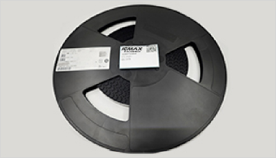
- Step1:Prepare product
-
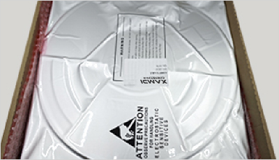
- Step2:Vacuum packaging
-
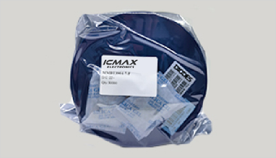
- Step3:Anti-static bag
-
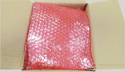
- Step4:Individual package
-
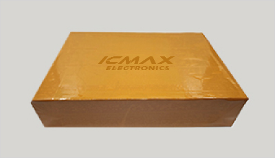
- Step5:Packaging box
-
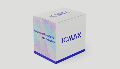
- Step6:Barcode shipping label
Shipping starts at $40, but some countries will exceed $40. For example (South Africa, Brazil, India, Pakistan, Israel, etc.)
The basic freight (for package ≤0.5kg or corresponding volume) depends on the time zone and country.
Currently, our products are shipped through DHL, FedEx, SF, and UPS.
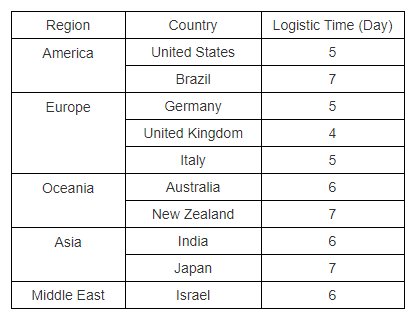
Delivery TimeOnce the goods are shipped, estimated delivery time depends on the shipping methods you chose:
FedEx International, 5-7 business days.
The following are some common countries' logistic time.
- Hot Sale
- Related Categories
- Include Parts
- Popular Search
The following parts include "NCE30P30K" in Silicon Labs NCE30P30K.
- Part Number
- Manufacturer
- Package
- Description
- NCE2305A NCEPower NCE30P30K — 30V/30A P-Channel Power MOSFET (TO-252-2L)The NCE30P30K is a -30V/-30A P-Channel trench MOSFET in TO-252-2L (DPAK) — 18mΩ max at 10V (typ 13mΩ), 31.2nC gate charge, and a spec sheet that answers the questions the sibling…
- NCE2305 NCEPower NCE30P30K — 30V/30A P-Channel Power MOSFET (TO-252-2L)The NCE30P30K is a -30V/-30A P-Channel trench MOSFET in TO-252-2L (DPAK) — 18mΩ max at 10V (typ 13mΩ), 31.2nC gate charge, and a spec sheet that answers the questions the sibling…
- NCE3401 : P-Channel 30V -4.2A Power MOSFET SOT-23 NCEPower NCE30P30K — 30V/30A P-Channel Power MOSFET (TO-252-2L)The NCE30P30K is a -30V/-30A P-Channel trench MOSFET in TO-252-2L (DPAK) — 18mΩ max at 10V (typ 13mΩ), 31.2nC gate charge, and a spec sheet that answers the questions the sibling…
- NCE9435 NCEPower NCE30P30K — 30V/30A P-Channel Power MOSFET (TO-252-2L)The NCE30P30K is a -30V/-30A P-Channel trench MOSFET in TO-252-2L (DPAK) — 18mΩ max at 10V (typ 13mΩ), 31.2nC gate charge, and a spec sheet that answers the questions the sibling…
- NCE30P12S NCEPower NCE30P30K — 30V/30A P-Channel Power MOSFET (TO-252-2L)The NCE30P30K is a -30V/-30A P-Channel trench MOSFET in TO-252-2L (DPAK) — 18mΩ max at 10V (typ 13mΩ), 31.2nC gate charge, and a spec sheet that answers the questions the sibling…
- NCE30P25S NCEPower NCE30P30K — 30V/30A P-Channel Power MOSFET (TO-252-2L)The NCE30P30K is a -30V/-30A P-Channel trench MOSFET in TO-252-2L (DPAK) — 18mΩ max at 10V (typ 13mΩ), 31.2nC gate charge, and a spec sheet that answers the questions the sibling…
- NCE30P30K NCEPower NCE30P30K — 30V/30A P-Channel Power MOSFET (TO-252-2L)The NCE30P30K is a -30V/-30A P-Channel trench MOSFET in TO-252-2L (DPAK) — 18mΩ max at 10V (typ 13mΩ), 31.2nC gate charge, and a spec sheet that answers the questions the sibling…
- NCE30P30G NCEPower NCE30P30K — 30V/30A P-Channel Power MOSFET (TO-252-2L)The NCE30P30K is a -30V/-30A P-Channel trench MOSFET in TO-252-2L (DPAK) — 18mΩ max at 10V (typ 13mΩ), 31.2nC gate charge, and a spec sheet that answers the questions the sibling…
- NCE30P50G NCEPower NCE30P30K — 30V/30A P-Channel Power MOSFET (TO-252-2L)The NCE30P30K is a -30V/-30A P-Channel trench MOSFET in TO-252-2L (DPAK) — 18mΩ max at 10V (typ 13mΩ), 31.2nC gate charge, and a spec sheet that answers the questions the sibling…
- NCE2309 — P-Channel 60V/1.6A Enhancement Mode Power MOSFET (SOT-23) NCEPower NCE30P30K — 30V/30A P-Channel Power MOSFET (TO-252-2L)The NCE30P30K is a -30V/-30A P-Channel trench MOSFET in TO-252-2L (DPAK) — 18mΩ max at 10V (typ 13mΩ), 31.2nC gate charge, and a spec sheet that answers the questions the sibling…
The following parts are popular search parts in Test and Measurement.
Inventory:50,000
Please send an inquiry. Send us your inquiry, and we will respond immediately.

- 1500+ Daily average RFQ Volume

- 20,000.000 Standard Product Unit

- 1800+ Worldwide Manufacturers

- 15,000+ In-stock Warehouse


