


NCEPower NCE30P30G

- Part No.:
- NCE30P30G
- Manufacturer:
- NCEPower
- Category:
- P-Channel MOSFETs
- Package:
- Description:
- NCE30P30G — 30V/30A P-Channel Power MOSFET (DFN5×6-8L)The NCE30P30G is a -30V/-30A P-Channel trench MOSFET in DFN5×6-8L — 10mΩ max at 10V (typ 7.4mΩ), 15mΩ max at 4.5V, 81.3nC gate charge, from Wuxi NCE Power, data…
- Quantity:
-
Unit Price:$0
Ext Price:$0
- Payment:
-

- Shipping:
-


NCE30P30G Information
- Specifications
- Product Details
- Comparison
- Tags
- Product attributes
- Attribute value
- Manufacturer:
- NCEPower
- Package/Case:
- Series:
- Packaging:
- DFN5*6
- Product Status:
- Production
- FET Type:
- Industrial grade
- Technology:
- Trench
- Drain to Source Voltage (Vdss):
- P
- Current - Continuous Drain (Id) @ 25°C:
- -30
- Drive Voltage (Max Rds On, Min Rds On):
- -30
- Rds On (Max) @ Id, Vgs:
- -1.6
- Vgs(th) (Max) @ Id:
- 7.4
- Gate Charge (Qg) (Max) @ Vgs:
- 12
- Vgs (Max):
- 10.6
- Input Capacitance (Ciss) (Max) @ Vds:
- 15
- FET Feature:
- Power Dissipation (Max):
- Operating Temperature:
- ±20
- Grade:
- 4222
- Qualification:
- 81
- Mounting Type:
- 45
- Supplier Device Package:
- 供应商设备封装:
- 供应商设备封装:
- 控制特性:
- 认证机构:
- 标准编号:
- Current Rating (Amps):
- param_30:
NCE30P30G — 30V/30A P-Channel Power MOSFET (DFN5×6-8L)
The NCE30P30G is a -30V/-30A P-Channel trench MOSFET in DFN5×6-8L — 10mΩ max at 10V (typ 7.4mΩ), 15mΩ max at 4.5V, 81.3nC gate charge, from Wuxi NCE Power, datasheet v1.0.
From what we see across Shenzhen lots (2025–2026), this DFN die is the part designers move to when an SOP-8 30P part's continuous load passes roughly 10-12A: the heat has nowhere to go in a plastic SO-8 body, and the DFN's bottom pad is the exit.
The spec that doesn't get quoted enough: this datasheet publishes no EAS row and no 100°C current row — and the 80W envelope is a case rating that only exists if the pad is soldered to real copper.
Buy the 30P30G for the family's best case thermal path (RθJC 1.56°C/W), a real 4.5V drive row, and an honest spec sheet — then design the pad and the gate rail, because both are the rating.
What Are the Technical Specifications of NCE30P30G?
| Parameter | Value |
|---|---|
| Type | P-Channel Enhancement Mode Power MOSFET (Trench) |
| Package | DFN5×6-8L (8 leads + exposed drain pad) |
| Drain-Source Voltage (VDS) | -30V (typ -33V) |
| Gate-Source Voltage (VGS) | ±20V max |
| Continuous Drain Current (ID) | -30A @ TC = 25°C |
| Continuous Drain Current @ 100°C | Not published — see note below |
| Pulsed Drain Current (IDM) | -160A (pulse width limited by Tj) |
| On-Resistance RDS(on) @ 10V | 7.4mΩ typ / 10mΩ max (ID = -15A) |
| On-Resistance RDS(on) @ 4.5V | 11mΩ typ / 15mΩ max (ID = -10A) |
| Gate Threshold Voltage (VGS(th)) | -1.0V to -2.2V (typ -1.5V) |
| Forward Transconductance (gfs) | 30S typ (VDS = -5V, ID = -15A) |
| Max Power Dissipation (PD) | 80W (TC = 25°C) |
| Thermal Resistance RθJC | 1.56°C/W |
| Total Gate Charge (Qg) | 81.3nC (VDS = -15V, ID = -15A, VGS = -10V) |
| Gate-Source Charge (Qgs) / Gate-Drain (Qgd) | 13.8nC / 8.3nC |
| Input Capacitance (Ciss) | 4222pF (VDS = -15V) |
| Output / Reverse Transfer Capacitance | Coss 480.5pF / Crss 448.6pF |
| Switching Times | td(on) 15ns / tr 11ns / td(off) 44ns / tf 21ns (VDD = -15V, RGEN = 3Ω) |
| Body Diode Forward Voltage (VSD) | -1.2V (IS = -30A) |
| Body Diode Recovery (trr) | Not published |
| Single Pulse Avalanche Energy (EAS) | Not published — "100% UIS TESTED" only |
| Operating Junction Temperature | -55°C to +150°C |
Key numbers that matter: per the NCE30P30G datasheet (v1.0), the 10V row is guaranteed at a -15A test current, and the 4.5V row — 15mΩ max at -10A — is a real guarantee, not a marketing line.
That puts it in the same 4.5V-drive class as the SOP-8 line (the 30P25S guarantees 14mΩ max at 4.5V). What the DFN adds is not drive — it is the heat path.
But the same table is what you must read twice: no ID at 100°C, no trr, no EAS number — only the feature line "100% UIS TESTED".
The 30P30K sibling publishes EAS 169mJ; the 30P50G publishes 300mJ. This die's avalanche budget is not on paper, so treat unclamped events as unquantified and clamp them.
Two dies, one -30A sticker — RDS(on) max at 10V (datasheet):
The G die is the bigger, lower-resistance die of the 30A pair — and it charges for it in gate charge:
Total gate charge Qg (datasheet):
Same current class, opposite philosophies: 1.8× lower RDS(on) for 2.6× the gate charge. Pick by your drive budget, not by the sticker.
What does a 30A board actually need from its high-side switch? The driver and the pad decide — not the sticker.
When Should You Use (and NOT Use) the NCE30P30G?
✅ Use NCE30P30G when:
- High-side switching where the continuous load is real, 8-15A, on a 12-18V rail. The DFN pad with 2oz copper and vias gives this die a case-to-board path the SOP-8 line cannot reach — RθJC 1.56°C/W is the family's best number.
- 4.5V-drive designs. The guaranteed 15mΩ max at 4.5V/-10A makes 5V-logic drive defensible — same drive class as the 30P25S (14mΩ max), with a pad that conducts better.
- Load switches and PWM on battery rails up to 4S Li-ion (~16.8V). On-state VGS stays inside the ±20V limit with real margin.
- Power-OR / input-switch positions that want a P-ch instead of a load-switch IC. At this current class the discrete P-ch + 2N3904 level-shift is still the cheaper BOM — when the switching speed is modest.
- Replacing an SOP-8 30P part on the same board when the layout can change. Same family, same drive logic, a pad that actually conducts heat.
❌ Don't use NCE30P30G when:
- Your rail is 24V and the gate is pulled to ground to turn on. On-state VGS would be about -24V against a ±20V rating. Use a zener clamp (18V) between gate and source, or stay at or below ~18V rails.
- You need a guaranteed avalanche or inductive-spike budget. No EAS value is published for this die. The 30P30K (169mJ) and 30P50G (300mJ) publish numbers; this one does not — clamp your flyback energy.
- 3.3V-logic direct drive. The -1.0 to -2.2V threshold conducts at 3.3V, but RDS(on) is only guaranteed at 4.5V and 10V. Level-shift with an NPN or N-MOSFET — don't trust 3.3V for 15mΩ.
- Fast PWM from a plain pull-up resistor. 81.3nC against a 100kΩ pull-up switches in the low kilohertz at best. Push-pull or a driver IC for real PWM rates.
- Hand-soldering this part on a big copper pour. The very pad that cools it sinks your hot-air heat; DFN5×6 rework on large planes needs preheat or a hot plate (real forum-reported pain).
What Are the Alternatives to NCE30P30G?
| Model | Type | Key Difference | Best For |
|---|---|---|---|
| NCE30P50G | P-Ch, DFN 5x6 EP | Same footprint, -50A/-200A pulse, 7mΩ max, EAS 300mJ published — but PD 35W and RθJC 3.6°C/W | 50A-class loads where the pad is big enough to matter |
| NCE30P30K | P-Ch, TO-252-2L | Same -30A sticker, 18mΩ max, only 31.2nC, EAS 169mJ, ID -21.2A at 100°C | Lower gate-charge budgets and tab-soldered thermal paths |
| NCE30P25S | P-Ch, SOP-8 | 25A, 9mΩ max at 10V, no 4.5V row, 98.9nC — the SO-8 thermal wall at ~10A continuous | Drop-in on existing SO-8 layouts at modest current |
| N-ch + high-side driver | N-Ch + driver IC | Halves conduction loss at the same die cost, adds a driver and level-shift | Above ~20A continuous where P-ch economics break |
The 30A decision in one line: the G is the bigger die with the better case thermal path; the K is the smaller die with the lighter gate.
Here's the thing to check before buying: your pad and your driver.
If the board has 2oz copper and a push-pull stage, the G's 10mΩ earns its 81.3nC.
If the gate comes from a weak source, or the board is 1oz with no vias, the K is the honest answer.
Above 20A continuous, an N-ch plus driver stops being optional.
The pad is the rating: 80W case-rated at RθJC 1.56°C/W assumes the pad is soldered to copper that carries the heat away. No RθJA is published — the honest continuous number is set by your pad, vias and airflow, not the sticker.
High-side load switch, the P-ch way: the pull-up must reference the source rail (BAT+), not logic ground — otherwise the FET never fully turns off.
The 2N3904 pulls the gate to ground to turn on. On a 24V rail that would exceed ±20V, so clamp with an 18V zener between gate and source.
For PWM above a few kilohertz, replace the 100k pull-up with a push-pull stage — 81.3nC against 100kΩ is an RC switch, not a gate drive.
What Are the Typical Applications of NCE30P30G?
High-current load switches on 2S-4S battery rails. The datasheet's own application list starts with battery and load switching. On 4S Li-ion (up to ~16.8V) the on-state VGS stays inside ±20V, and the DFN pad handles the continuous current an SO-8 body cannot.
Power-OR and input-switch positions in 12-18V systems. Two P-ch parts back-to-back replace a load-switch IC below ~15A continuous, when switching speed is modest — the discrete BOM wins on cost and the 10mΩ on loss.
UPS and 24V-class PWM where the rail is clamped. P-ch high-side PWM in inverters and UPS modules is a listed application — with an 18V gate clamp and a driver, not a pull-up.
Board-level upgrades from the SOP-8 30P line. When a 30P25S board runs hot past ~10A continuous and the layout can change, the same family in DFN5×6 is the shortest engineering path — same drive logic, a pad that actually leaves.
Why Buy NCE30P30G from ICMASS?
Every lot batch-tested at the 10V drive point. We test RDS(on) at 10V/-15A against the 10mΩ max and sample-test the 4.5V row — because the 4.5V guarantee is the reason most buyers pick this die over the SOP-8 line.
Family cross-reference support. G, K, or 50G? Send us rail voltage, continuous load, drive source and board copper — we'll tell you which die philosophy your design actually needs, including when the honest answer is an N-ch plus driver.
Pad and land-pattern verification on request. We verify the DFN5×6 pad map against the datasheet figure before we advise layouts, and confirm your lot's marking and RDS(on) before volume orders.
Same-day dispatch, 5-10 days worldwide. Orders before 15:00 CST ship same day via DHL or FedEx. For volume, we source directly from the NCE factory line.
Frequently Asked Questions About NCE30P30G
Q1: What's the real difference between NCE30P30G and NCE30P30K?
A: Different dies with the same -30A sticker. The G (DFN5×6) runs 10mΩ max with 81.3nC; the K (TO-252) runs 18mΩ max with only 31.2nC. Lower resistance costs 2.6× the gate charge. Pick the G when the driver is strong and the pad is real copper; pick the K for lighter drive and a tab-soldered heat path.
Q2: Can I switch a 24V rail with a ±20V gate rating?
A: Only with a clamp. Turning on pulls the gate to ground, so VGS reaches about -24V on a 24V rail — above the ±20V max. Add an 18V zener between gate and source, or keep the rail at or below ~18V. On 4S Li-ion (~16.8V) the margin is real and no clamp is needed.
Q3: Can a 3.3V MCU pin drive it directly?
A: It conducts, but nothing is guaranteed. The threshold band is -1.0 to -2.2V, so 3.3V turns the channel on — but RDS(on) is only guaranteed at 4.5V and 10V. For a guaranteed 15mΩ, level-shift with an NPN or N-MOSFET and drive the gate from 4.5V or more.
Q4: Why does my high-side switch stay on when the MCU resets or is unpowered?
A: The gate is not at the source rail. A P-ch turns off only when VGS is near zero — the pull-up must go to BAT+ (source), not to logic. During reset the gate holds its charge and the FET stays on; a 100kΩ pull-up to the source rail gives a defined off state. Beware a driver whose unpowered supply back-feeds through the pull-up — a real forum-reported failure mode.
Q5: What does the DFN pad need to carry 30A?
A: Copper, vias, and a grid stencil. The pad is the drain and the entire heat path. Use 2oz top copper under the pad, 0.2-0.3mm thermal vias at ~1mm pitch (filled or plugged to stop solder wicking), and a stencil grid of ~70-75% open area — a solid aperture raises voiding, and voids above ~35% can lift thermal resistance by 18-22%.
Q6: What's the real continuous current on a board?
A: Whatever your pad allows — and this datasheet publishes no 100°C current row and no RθJA to lean on. The 80W rating is case-bound at RθJC 1.56°C/W. On a good 2oz board with vias, honest continuous current lands far below the 30A sticker; on a skimpy pad it lands embarrassingly low. Measure with a thermocouple before production.
Q7: What about avalanche or inductive spikes?
A: This die publishes no EAS number — clamp the energy. The datasheet claims 100% UIS testing but lists no avalanche value, unlike the 30P30K (169mJ) and 30P50G (300mJ) siblings. For unclamped inductive loads, add a clamp or snubber and treat the budget as unquantified.
Q8: What gate drive do I need for PWM?
A: Push-pull or a driver IC above a few kilohertz. Qg is 81.3nC. A 100kΩ pull-up plus 81.3nC forms an RC switch that settles in the low kilohertz, sitting in the linear region meanwhile — that is how P-ch PWM boards burn. A push-pull stage or driver IC is the difference between switching and simmering.
Q9: How do I verify a genuine NCE30P30G?
A: Measure RDS(on) at 10V/-15A and the threshold. A genuine part reads within 10mΩ max and VGS(th) in the -1.0 to -2.2V band. Confirm the DFN5×6 footprint and marking too — a relabeled smaller die fails the milliohm check at the -15A test current.
| Image |

|
| Part Number | NCE30P30G |
| Manufacturer | NCEPower |
| Package/Case | |
| Series | |
| Packaging | DFN5*6 |
| Product Status | Production |
| FET Type | Industrial grade |
| Technology | Trench |
| Drain to Source Voltage (Vdss) | P |
| Current - Continuous Drain (Id) @ 25°C | -30 |
| Drive Voltage (Max Rds On, Min Rds On) | -30 |
| Rds On (Max) @ Id, Vgs | -1.6 |
| Vgs(th) (Max) @ Id | 7.4 |
| Gate Charge (Qg) (Max) @ Vgs | 12 |
| Vgs (Max) | 10.6 |
| Input Capacitance (Ciss) (Max) @ Vds | 15 |
| FET Feature | |
| Power Dissipation (Max) | |
| Operating Temperature | ±20 |
| Grade | 4222 |
| Qualification | 81 |
| Mounting Type | 45 |
| Supplier Device Package | |
| 供应商设备封装 | |
| 供应商设备封装 | |
| 控制特性 | |
| 认证机构 | |
| 标准编号 | |
| Current Rating (Amps) | |
| param_30 |
User Guide
- Purchase & Inquiry
- Package
- Shipping Information
- Customer Review
You may place an order without registering to IC-MAX.COM
We strongly suggest you sign in before purchasing as you can track your order in real time.
For your convenience, we accept multiple payment methods in USD, including PayPal, Credit Card, and wire transfer.
RFQ (Request for Quotations)
It is recommended to request for quotations to get the latest prices and inventories about the part.
Our sales will reply to your request by email within 24 hours.
1. You'll receive an order information email in your inbox. (Please remember to check the spam folder if you didn't hear from us).
2. Since inventories and prices may fluctuate to some extent, the sales manager is going to reconfirm the order and let you know if there are any updates.
-
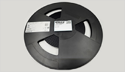
- Step1:Prepare product
-
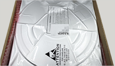
- Step2:Vacuum packaging
-
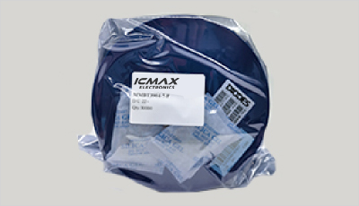
- Step3:Anti-static bag
-
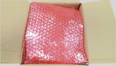
- Step4:Individual package
-
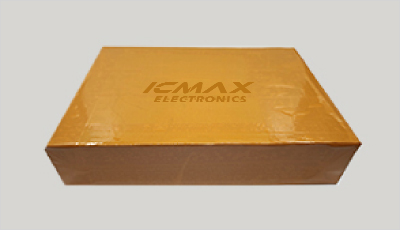
- Step5:Packaging box
-
- Step6:Barcode shipping label
Shipping starts at $40, but some countries will exceed $40. For example (South Africa, Brazil, India, Pakistan, Israel, etc.)
The basic freight (for package ≤0.5kg or corresponding volume) depends on the time zone and country.
Currently, our products are shipped through DHL, FedEx, SF, and UPS.
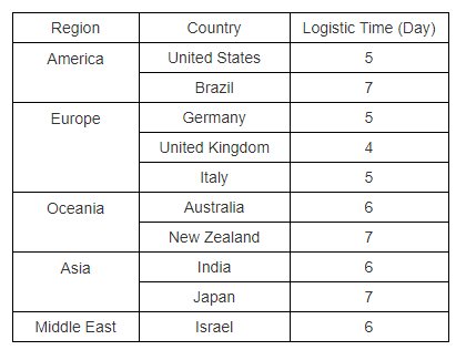
Delivery TimeOnce the goods are shipped, estimated delivery time depends on the shipping methods you chose:
FedEx International, 5-7 business days.
The following are some common countries' logistic time.
- Hot Sale
- Related Categories
- Include Parts
- Popular Search
The following parts include "NCE30P30G" in Silicon Labs NCE30P30G.
- Part Number
- Manufacturer
- Package
- Description
- NCE2305A NCEPower NCE30P30G — 30V/30A P-Channel Power MOSFET (DFN5×6-8L)The NCE30P30G is a -30V/-30A P-Channel trench MOSFET in DFN5×6-8L — 10mΩ max at 10V (typ 7.4mΩ), 15mΩ max at 4.5V, 81.3nC gate charge, from Wuxi NCE Power, data…
- NCE2305 NCEPower NCE30P30G — 30V/30A P-Channel Power MOSFET (DFN5×6-8L)The NCE30P30G is a -30V/-30A P-Channel trench MOSFET in DFN5×6-8L — 10mΩ max at 10V (typ 7.4mΩ), 15mΩ max at 4.5V, 81.3nC gate charge, from Wuxi NCE Power, data…
- NCE3401 : P-Channel 30V -4.2A Power MOSFET SOT-23 NCEPower NCE30P30G — 30V/30A P-Channel Power MOSFET (DFN5×6-8L)The NCE30P30G is a -30V/-30A P-Channel trench MOSFET in DFN5×6-8L — 10mΩ max at 10V (typ 7.4mΩ), 15mΩ max at 4.5V, 81.3nC gate charge, from Wuxi NCE Power, data…
- NCE9435 NCEPower NCE30P30G — 30V/30A P-Channel Power MOSFET (DFN5×6-8L)The NCE30P30G is a -30V/-30A P-Channel trench MOSFET in DFN5×6-8L — 10mΩ max at 10V (typ 7.4mΩ), 15mΩ max at 4.5V, 81.3nC gate charge, from Wuxi NCE Power, data…
- NCE30P12S NCEPower NCE30P30G — 30V/30A P-Channel Power MOSFET (DFN5×6-8L)The NCE30P30G is a -30V/-30A P-Channel trench MOSFET in DFN5×6-8L — 10mΩ max at 10V (typ 7.4mΩ), 15mΩ max at 4.5V, 81.3nC gate charge, from Wuxi NCE Power, data…
- NCE30P25S NCEPower NCE30P30G — 30V/30A P-Channel Power MOSFET (DFN5×6-8L)The NCE30P30G is a -30V/-30A P-Channel trench MOSFET in DFN5×6-8L — 10mΩ max at 10V (typ 7.4mΩ), 15mΩ max at 4.5V, 81.3nC gate charge, from Wuxi NCE Power, data…
- NCE30P30K NCEPower NCE30P30G — 30V/30A P-Channel Power MOSFET (DFN5×6-8L)The NCE30P30G is a -30V/-30A P-Channel trench MOSFET in DFN5×6-8L — 10mΩ max at 10V (typ 7.4mΩ), 15mΩ max at 4.5V, 81.3nC gate charge, from Wuxi NCE Power, data…
- NCE30P30G NCEPower NCE30P30G — 30V/30A P-Channel Power MOSFET (DFN5×6-8L)The NCE30P30G is a -30V/-30A P-Channel trench MOSFET in DFN5×6-8L — 10mΩ max at 10V (typ 7.4mΩ), 15mΩ max at 4.5V, 81.3nC gate charge, from Wuxi NCE Power, data…
- NCE30P50G NCEPower NCE30P30G — 30V/30A P-Channel Power MOSFET (DFN5×6-8L)The NCE30P30G is a -30V/-30A P-Channel trench MOSFET in DFN5×6-8L — 10mΩ max at 10V (typ 7.4mΩ), 15mΩ max at 4.5V, 81.3nC gate charge, from Wuxi NCE Power, data…
- NCE2309 — P-Channel 60V/1.6A Enhancement Mode Power MOSFET (SOT-23) NCEPower NCE30P30G — 30V/30A P-Channel Power MOSFET (DFN5×6-8L)The NCE30P30G is a -30V/-30A P-Channel trench MOSFET in DFN5×6-8L — 10mΩ max at 10V (typ 7.4mΩ), 15mΩ max at 4.5V, 81.3nC gate charge, from Wuxi NCE Power, data…
The following parts are popular search parts in Test and Measurement.
Inventory:50,000
Please send an inquiry. Send us your inquiry, and we will respond immediately.

- 1500+ Daily average RFQ Volume

- 20,000.000 Standard Product Unit

- 1800+ Worldwide Manufacturers

- 15,000+ In-stock Warehouse


