


NCEPower NCE30P12S

- Part No.:
- NCE30P12S
- Manufacturer:
- NCEPower
- Category:
- P-Channel MOSFETs
- Package:
- Description:
- NCE30P12S — -30V/-12A P-Channel Power MOSFET (SOP-8)The NCE30P12S is a -30V, -12A P-Channel enhancement-mode power MOSFET in SOP-8 from Wuxi NCE Power — the high-current step above the 9435 family. Trench cell, logic-level gate drive down to -4…
- Quantity:
-
Unit Price:$0
Ext Price:$0
- Payment:
-

- Shipping:
-


NCE30P12S Information
- Specifications
- Product Details
- Comparison
- Tags
- Product attributes
- Attribute value
- Manufacturer:
- NCEPower
- Package/Case:
- Series:
- Packaging:
- SOP-8
- Product Status:
- Production
- FET Type:
- Industrial grade
- Technology:
- Trench
- Drain to Source Voltage (Vdss):
- P
- Current - Continuous Drain (Id) @ 25°C:
- -30
- Drive Voltage (Max Rds On, Min Rds On):
- -12
- Rds On (Max) @ Id, Vgs:
- -1.5
- Vgs(th) (Max) @ Id:
- 11.5
- Gate Charge (Qg) (Max) @ Vgs:
- 15
- Vgs (Max):
- 18
- Input Capacitance (Ciss) (Max) @ Vds:
- 25
- FET Feature:
- Power Dissipation (Max):
- Operating Temperature:
- ±20
- Grade:
- 1750
- Qualification:
- 24
- Mounting Type:
- 3
- Supplier Device Package:
- 供应商设备封装:
- 供应商设备封装:
- 控制特性:
- 认证机构:
- 标准编号:
- Current Rating (Amps):
- param_30:
NCE30P12S — -30V/-12A P-Channel Power MOSFET (SOP-8)
The NCE30P12S is a -30V, -12A P-Channel enhancement-mode power MOSFET in SOP-8 from Wuxi NCE Power — the high-current step above the 9435 family. Trench cell, logic-level gate drive down to -4.5V, and RDS(on) of 13mΩ max @ -10V.
From what we see across Shenzhen lots (2025–2026), the 30P series is where 9435-family designs graduate when the load passes 4–5A. Same SOP-8 socket, same pinout — but the die carries 2.5× the current.
The most common field complaint we hear: engineers treat the -12A rating as a continuous promise. It isn't.
That number is measured at TA = 25°C with ideal copper; at 13mΩ the real continuous current on a typical board is closer to 8A. Get the thermal budget right and this part is a workhorse — ignore it and it's a heater.
What Are the Technical Specifications of NCE30P12S?
| Parameter | Value |
|---|---|
| Type | P-Channel Enhancement Mode Power MOSFET (Trench) |
| Package | SOP-8, RoHS / lead-free, tape & reel (4000/reel) |
| Drain-Source Voltage (VDS) | -30V |
| Gate-Source Voltage (VGS) | ±20V |
| Continuous Drain Current (ID) | -12A @ TA = 25°C |
| Continuous Drain Current (ID) | -8.4A @ TA = 100°C |
| Pulsed Drain Current (IDM) | -48A |
| On-Resistance RDS(on) @ -10V | 11.5mΩ typ / 13mΩ max (ID=-10A) |
| On-Resistance RDS(on) @ -4.5V | 15mΩ typ / 21mΩ max (ID=-7A) |
| Gate Threshold Voltage (VGS(th)) | -1.0V to -2.2V (typ -1.5V) |
| Max Power Dissipation (PD) | 3W @ TA = 25°C / 1.3W @ 100°C |
| Thermal Resistance RθJA | 41.67°C/W |
| Total Gate Charge (Qg) | 24nC @ VGS=-10V |
| Input Capacitance (Ciss) | 1.75nF typ |
| Single Pulse Avalanche Energy (EAS) | 231mJ |
| Operating Junction Temperature | -55°C to +150°C |
Key numbers that matter: per the NCE30P12S datasheet, RDS(on) is guaranteed at -4.5V and -10V — the same two drive points as the whole 30P family.
At -10V the part reaches 13mΩ max; at -4.5V it climbs to 21mΩ — a 60% jump. But why does that matter? At 10A, the difference is 1.3W vs 2.1W of heat, and SOP-8 only sheds so much.
The -48A pulse rating and 231mJ avalanche energy let it shrug off capacitor inrush and inductive load spikes that kill smaller P-Channel parts.
When Should You Use (and NOT Use) the NCE30P12S?
✅ Use NCE30P12S when:
- High-side load switching at 4–8A. Battery tools, power banks, gimbal and drone boards — the -30V rating covers 1S to 6S Li-ion with margin for inductive spikes.
- Reverse polarity protection above 2A. Body diode blocks the reversed supply, then the channel takes over at 13mΩ instead of a diode's 0.4–0.6V drop. At 5A that's 0.33W vs 2.5W.
- 4.5V logic-level gate drive. A 5V MCU rail or a small NPN level shifter switches it fully — no gate driver IC needed.
- Upgrade from a 9435-family part. Same SOP-8 pinout, same -30V rating; the 30P12S carries 2.5× the current with a quarter of the RDS(on).
- PWM fan or motor control up to tens of kHz. The 24nC gate charge and 48A pulse rating handle load-switch speeds comfortably.
❌ Don't use NCE30P12S when:
- You plan to draw a true 12A continuously. That rating is at TA = 25°C with generous copper. At 13mΩ and 12A you dissipate 1.9W — a 78°C junction rise. Step up to NCE30P25S (6.4mΩ typ) or a TO-252 P-Channel.
- Driving from a 3.3V-only rail with no level shifter. RDS(on) is not specified below -4.5V; at -3.3V the die is partially enhanced and resistance climbs 2–3×. Add the NPN stage — it's two components.
- Gate voltages above -20V. A 24V rail with the gate pulled to ground puts 24V across VGS — instant overstress. Add a Zener clamp between gate and source.
- High-frequency switching stages. 24nC gate charge makes this a load switch, not a 100kHz+ synchronous-rectifier FET. Pick a lower-Qg part and a proper driver for that.
What Are the Alternatives to NCE30P12S?
| Model | Type | Key Difference | Best For |
|---|---|---|---|
| NCE30P15S | P-Ch, SOP-8 | -15A, 12mΩ @ -10V, 3.1W | Same-socket upgrade; +25% current headroom |
| NCE30P25S | P-Ch, SOP-8 | -25A, 6.4mΩ typ @ -10V, 3.5W | True 10A+ continuous; roughly half the heat |
| AO4407A | P-Ch, SOP-8 | -12A, 11mΩ, 4.5V drive (AOS) | Direct pin-compatible competitor, slightly lower RDS(on) |
| IRF9328 | P-Ch, SOP-8 | -30V, 10mΩ @ -10V, 2.5W (UMW) | Lowest RDS(on) at the same voltage |
| IRF7240 | P-Ch, SO-8 | -40V, 13mΩ, 3.5W (Infineon) | Extra voltage headroom on noisy 24V rails |
| SI4435DY | P-Ch, SOP-8 | -8.8A, 26mΩ, Vishay classic | Branded low-current drop-in; not for 8A+ |
The 30V P-Channel SOP-8 decision in one line: below 5A any 9435-family part works; from 5–8A the 30P12S is the sweet spot; above 8A continuous, go straight to the 30P25S.
In our experience (2025–2026), designs that start on the 9435 and survive a few revisions end up here — the jump to 13mΩ cuts conduction loss roughly 4× versus the 53mΩ original at the same current.
How do you choose the upgrade step? Match it to how long the load stays at peak current — 5A bursts, an 8A continuous rail, and a true 12A design all land on different parts.
SOP-8 pinout: pins 1–3 are Source, pin 4 is Gate, pins 5–8 are Drain — identical to the 9435 family, so the 30P12S drops into the same board without a layout change.
High-side switch with level shifter: gate pulled up to VIN through 10kΩ (off), GPIO drives an NPN which pulls the gate to ground to enable.
On rails above 20V, add a 12V Zener clamp across gate-source to keep VGS inside ±20V. This is the two-component fix forums converge on for MCU-driven P-Channel loads.
RDS(on) max @ -10V drive — lower is less heat at the same current:
At 8A, the difference between 13mΩ and 6.4mΩ (typ) is 0.83W vs 0.41W of heat — the 30P25S upgrade matters the moment your load passes 8A continuous.
What Are the Typical Applications of NCE30P12S?
Power bank output stage: The 30P12S sits between the 2S Li-ion pack and the USB output. Gate driven from the charge/discharge MCU through an NPN; the -48A pulse rating absorbs hot-plug inrush from the load's bulk capacitors without a soft-start circuit.
Battery tool high-side switch: In a cordless tool or portable instrument drawing 5–8A bursts, the 30P12S replaces a 9435-family part without a layout change. Off-state leakage is -1µA max — battery drain through the switch is negligible.
Reverse polarity protection: Connected source-to-load, drain-to-supply, the body diode blocks a reversed battery and the channel conducts at 13mΩ after the gate is pulled negative. At 5A the drop drops from ~0.4V (Schottky) to ~65mV.
Drone and gimbal power gating: Camera gimbals and drone peripherals need clean 5–12V rails switched at load-switch speeds. The 4.5V drive spec matches a 5V rail directly; the 231mJ avalanche rating handles motor back-EMF spikes.
Why Buy NCE30P12S from ICMASS?
Every lot tested for the two specs that matter. We batch-test VGS(th) and RDS(on) at -4.5V and -10V on 30P12S parts before they ship. A remarked lower-current die passes a visual check but fails the RDS(on) measurement by 2–3×.
Cross-reference support for the whole 30V P-Channel line. Not sure whether your board wants the 30P12S, 30P15S, 30P25S, or AO4407A? Send us your load current, rail voltage, and gate drive — we'll tell you which part the design actually needs.
BOM consolidation for battery products. The same portable-device BOM usually carries a battery charger (TP4056), a boost or buck converter (XL6009, LM2596), and the 30P12S load switch. One shipment from Shenzhen covers the whole power section.
Same-day dispatch, 5–10 days worldwide. Orders before 15:00 CST ship same day via DHL or FedEx. For volume orders, we source directly from the NCE factory line.
Frequently Asked Questions About NCE30P12S
Q1: Is NCE30P12S a drop-in replacement for AO4407?
A: Yes — same SOP-8 pinout, same -30V rating, same 4.5V drive points. Pins 1–3 Source, 4 Gate, 5–8 Drain on both. The 30P12S is 13mΩ max vs the AO4407A's 11mΩ — within 20%, no thermal surprise at typical loads. For a true 12A continuous design, both need the same PCB copper work.
Q2: My P-Channel high-side switch stays on no matter what the GPIO does — why?
A: The gate is not being pulled to the source potential, so the channel never turns off. A GPIO reaching only 3.3V or 5V cannot cut off a P-Channel on a 12V rail — VGS stays above threshold. The forum-standard fix: an NPN level shifter pulls the gate to ground to enable, and a 10kΩ pull-up between gate and source pulls it to VIN to disable. A swapped source/drain (body diode conducting) looks identical.
Q3: Can I drive NCE30P12S directly from a 3.3V MCU pin?
A: It will switch on, but RDS(on) is not specified below -4.5V. VGS(th) is typ -1.5V, so the channel conducts — but at -3.3V the die is only partially enhanced and resistance runs 2–3× the -4.5V value. For a 1–2A load with headroom it works; for 5A+ add the two-component NPN level shifter.
Q4: Can an SOP-8 really carry 12A continuous?
A: Not reliably — the -12A rating is at TA = 25°C with ideal copper. At 13mΩ max, 12A means 1.9W — a 78°C junction rise with the datasheet RθJA of 41.67°C/W. The datasheet itself derates to -8.4A at 100°C. With generous drain-pin copper pours, plan for ~8A continuous; beyond that step to the 30P25S.
Q5: My MOSFET burns out in a 24V system — what am I missing?
A: Check the gate voltage. VGS is rated ±20V, so pulling the gate to ground on a 24V rail puts 24V across gate-to-source — instant overstress. Add a 12V Zener clamp between gate and source, or a resistor divider, so the gate never sees more than -20V. This is the most common P-Channel failure mode reported on the forums.
Q6: NCE30P12S vs NCE30P25S — which should I use?
A: 30P12S up to ~8A continuous; 30P25S above that. Both are -30V SOP-8 P-Channel parts with the same pinout. The 25S drops RDS(on) from 13mΩ to 6.4mΩ typ — roughly half the heat at any current. At 8A that's the difference between 0.83W and 0.41W, which decides whether the SOP-8 stays cool.
Q7: Can I use the NCE30P12S for reverse polarity protection?
A: Yes — one of the best uses for a P-Channel part. Connect it source-to-load, drain-to-supply, so the body diode blocks the reversed supply; then the channel turns on and carries the load with millivolts of drop instead of a diode's 0.4–0.6V. The gate must pull to the load-side rail, not the supply side.
Q8: What gate pull-up and level-shift components should I use?
A: 10kΩ pull-up to VIN and an NPN (2N2222 or MMBT3904) with a 1kΩ base resistor. With Qg of 24nC, a 100kΩ pull-up forms a slow RC and the switch turns off in slow motion. Watch the backfeed: with the driver unpowered, the pull-up can keep the channel on through the driver's protection diodes — lower the pull-up or add a series diode to the driver rail.
Q9: My MCU resets when the load switch turns on — why?
A: Inrush into the capacitive load is dragging down the rail. The 30P12S can pulse -48A, so charging a few hundred microfarads can brown-out a weak supply. Add bulk bypass capacitance near the switch and consider a series resistor or soft-start for large capacitor banks.
Q10: How do I verify a genuine NCE30P12S?
A: Measure RDS(on) at -4.5V and -10V with a bench supply and milliohm meter. A genuine part reads near 15mΩ typ at -4.5V. Counterfeit parts remarked from smaller dies fail this check by 2–3× while passing a visual inspection — which is exactly why we batch-test this parameter before shipping.
| Image |

|
| Part Number | NCE30P12S |
| Manufacturer | NCEPower |
| Package/Case | |
| Series | |
| Packaging | SOP-8 |
| Product Status | Production |
| FET Type | Industrial grade |
| Technology | Trench |
| Drain to Source Voltage (Vdss) | P |
| Current - Continuous Drain (Id) @ 25°C | -30 |
| Drive Voltage (Max Rds On, Min Rds On) | -12 |
| Rds On (Max) @ Id, Vgs | -1.5 |
| Vgs(th) (Max) @ Id | 11.5 |
| Gate Charge (Qg) (Max) @ Vgs | 15 |
| Vgs (Max) | 18 |
| Input Capacitance (Ciss) (Max) @ Vds | 25 |
| FET Feature | |
| Power Dissipation (Max) | |
| Operating Temperature | ±20 |
| Grade | 1750 |
| Qualification | 24 |
| Mounting Type | 3 |
| Supplier Device Package | |
| 供应商设备封装 | |
| 供应商设备封装 | |
| 控制特性 | |
| 认证机构 | |
| 标准编号 | |
| Current Rating (Amps) | |
| param_30 |
User Guide
- Purchase & Inquiry
- Package
- Shipping Information
- Customer Review
You may place an order without registering to IC-MAX.COM
We strongly suggest you sign in before purchasing as you can track your order in real time.
For your convenience, we accept multiple payment methods in USD, including PayPal, Credit Card, and wire transfer.
RFQ (Request for Quotations)
It is recommended to request for quotations to get the latest prices and inventories about the part.
Our sales will reply to your request by email within 24 hours.
1. You'll receive an order information email in your inbox. (Please remember to check the spam folder if you didn't hear from us).
2. Since inventories and prices may fluctuate to some extent, the sales manager is going to reconfirm the order and let you know if there are any updates.
-
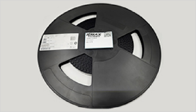
- Step1:Prepare product
-
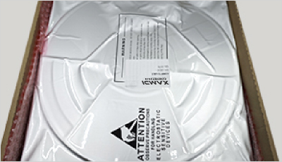
- Step2:Vacuum packaging
-
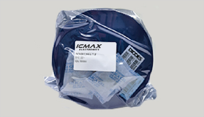
- Step3:Anti-static bag
-
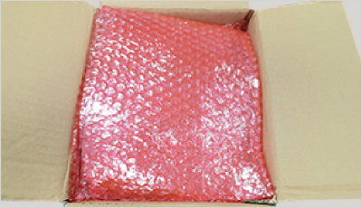
- Step4:Individual package
-
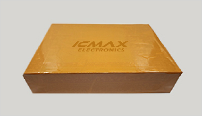
- Step5:Packaging box
-
- Step6:Barcode shipping label
Shipping starts at $40, but some countries will exceed $40. For example (South Africa, Brazil, India, Pakistan, Israel, etc.)
The basic freight (for package ≤0.5kg or corresponding volume) depends on the time zone and country.
Currently, our products are shipped through DHL, FedEx, SF, and UPS.
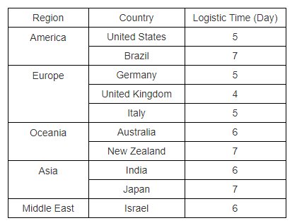
Delivery TimeOnce the goods are shipped, estimated delivery time depends on the shipping methods you chose:
FedEx International, 5-7 business days.
The following are some common countries' logistic time.
- Hot Sale
- Related Categories
- Include Parts
- Popular Search
The following parts include "NCE30P12S" in Silicon Labs NCE30P12S.
- Part Number
- Manufacturer
- Package
- Description
- NCE2305A NCEPower NCE30P12S — -30V/-12A P-Channel Power MOSFET (SOP-8)The NCE30P12S is a -30V, -12A P-Channel enhancement-mode power MOSFET in SOP-8 from Wuxi NCE Power — the high-current step above the 9435 family. Trench cell, logic-level gate drive down to -4…
- NCE2305 NCEPower NCE30P12S — -30V/-12A P-Channel Power MOSFET (SOP-8)The NCE30P12S is a -30V, -12A P-Channel enhancement-mode power MOSFET in SOP-8 from Wuxi NCE Power — the high-current step above the 9435 family. Trench cell, logic-level gate drive down to -4…
- NCE3401 : P-Channel 30V -4.2A Power MOSFET SOT-23 NCEPower NCE30P12S — -30V/-12A P-Channel Power MOSFET (SOP-8)The NCE30P12S is a -30V, -12A P-Channel enhancement-mode power MOSFET in SOP-8 from Wuxi NCE Power — the high-current step above the 9435 family. Trench cell, logic-level gate drive down to -4…
- NCE9435 NCEPower NCE30P12S — -30V/-12A P-Channel Power MOSFET (SOP-8)The NCE30P12S is a -30V, -12A P-Channel enhancement-mode power MOSFET in SOP-8 from Wuxi NCE Power — the high-current step above the 9435 family. Trench cell, logic-level gate drive down to -4…
- NCE30P12S NCEPower NCE30P12S — -30V/-12A P-Channel Power MOSFET (SOP-8)The NCE30P12S is a -30V, -12A P-Channel enhancement-mode power MOSFET in SOP-8 from Wuxi NCE Power — the high-current step above the 9435 family. Trench cell, logic-level gate drive down to -4…
- NCE30P25S NCEPower NCE30P12S — -30V/-12A P-Channel Power MOSFET (SOP-8)The NCE30P12S is a -30V, -12A P-Channel enhancement-mode power MOSFET in SOP-8 from Wuxi NCE Power — the high-current step above the 9435 family. Trench cell, logic-level gate drive down to -4…
- NCE30P30K NCEPower NCE30P12S — -30V/-12A P-Channel Power MOSFET (SOP-8)The NCE30P12S is a -30V, -12A P-Channel enhancement-mode power MOSFET in SOP-8 from Wuxi NCE Power — the high-current step above the 9435 family. Trench cell, logic-level gate drive down to -4…
- NCE30P30G NCEPower NCE30P12S — -30V/-12A P-Channel Power MOSFET (SOP-8)The NCE30P12S is a -30V, -12A P-Channel enhancement-mode power MOSFET in SOP-8 from Wuxi NCE Power — the high-current step above the 9435 family. Trench cell, logic-level gate drive down to -4…
- NCE30P50G NCEPower NCE30P12S — -30V/-12A P-Channel Power MOSFET (SOP-8)The NCE30P12S is a -30V, -12A P-Channel enhancement-mode power MOSFET in SOP-8 from Wuxi NCE Power — the high-current step above the 9435 family. Trench cell, logic-level gate drive down to -4…
- NCE2309 — P-Channel 60V/1.6A Enhancement Mode Power MOSFET (SOT-23) NCEPower NCE30P12S — -30V/-12A P-Channel Power MOSFET (SOP-8)The NCE30P12S is a -30V, -12A P-Channel enhancement-mode power MOSFET in SOP-8 from Wuxi NCE Power — the high-current step above the 9435 family. Trench cell, logic-level gate drive down to -4…
The following parts are popular search parts in Test and Measurement.
Inventory:50,000
Please send an inquiry. Send us your inquiry, and we will respond immediately.

- 1500+ Daily average RFQ Volume

- 20,000.000 Standard Product Unit

- 1800+ Worldwide Manufacturers

- 15,000+ In-stock Warehouse


