


UTC UT3N06G‑AB3‑R

- Part No.:
- UT3N06G‑AB3‑R
- Manufacturer:
- UTC
- Category:
- N-Channel MOSFETs
- Package:
- Description:
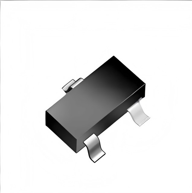
- UT3N06G-AB3-R – UTC N-Channel 60V 3A Enhancement Mode Power MOSFET Quick Answer The UT3N06G-AB3-R is an N-channel enhancement mode power MOSFET from Unisonic Technologies (UTC).
- Quantity:
-
Unit Price:$0
Ext Price:$0
- Payment:
-

- Shipping:
-


UT3N06G‑AB3‑R Information
- Specifications
- Product Details
- Comparison
- Tags
- Product attributes
- Attribute value
- Manufacturer:
- UTC
- Series:
- Package/Case:
- Packaging:
- SOT-23
- Product Status:
- Production
- FET Type:
- Industrial grade
- Technology:
- Trench
- Drain to Source Voltage (Vdss):
- N
- Current - Continuous Drain (Id) @ 25°C:
- 30
- Drive Voltage (Max Rds On, Min Rds On):
- 5.8
- Rds On (Max) @ Id, Vgs:
- 0.9
- Vgs(th) (Max) @ Id:
- 22
- Gate Charge (Qg) (Max) @ Vgs:
- 35
- Vgs (Max):
- 24
- Input Capacitance (Ciss) (Max) @ Vds:
- 41
- FET Feature:
- 28
- Power Dissipation (Max):
- 0℃ ~ +70℃
- Operating Temperature:
- ±12
- Grade:
- 820
- Qualification:
- 9.5
- Mounting Type:
- 1.4
- Supplier Device Package:
UT3N06G-AB3-R — 60V 3A N-Channel Power MOSFET (SOT-89) from UTC
The UT3N06G-AB3-R is a 60V, 3A N-channel enhancement-mode MOSFET in SOT-89 from Unisonic Technologies (UTC) — on-resistance of 90mΩ max at VGS=10V, gate threshold around 3V, and a package that survives nearly 700mW of continuous dissipation.
From what we see across Shenzhen lots (2025–2026), the UT3N06G is the default SOT-89 N-ch on load-switch and battery-path boards — the step between a SOT-23 part that can't carry current and a DPAK that costs twice as much board space.
The most common field complaint isn't a dead MOSFET — it's the 3A rating read as a promise. The SOT-89 package sets the real limit, and that limit is thermal, not electrical.
What Are the Technical Specifications of UT3N06G-AB3-R?
| Parameter | Value |
|---|---|
| Type | N-channel enhancement-mode power MOSFET |
| Package | SOT-89-3, halogen-free / lead-free |
| Drain-Source Voltage (VDSS) | 60V |
| Gate-Source Voltage (VGSS) | ±20V |
| Continuous Drain Current (ID) | 3A @ VGS=4.5V, TA=25°C |
| Pulsed Drain Current (IDM) | 12A (pulse ≤300µs, duty ≤2%) |
| On-Resistance (RDS(on)) | 90mΩ max @ VGS=10V, ID=3A; 120mΩ max @ 4.5V, ID=2A |
| Gate Threshold Voltage (VGS(th)) | 3V @ ID=250µA |
| Input Capacitance (Ciss) | 780pF @ VDS=25V, 1MHz |
| Total Gate Charge (Qg) | 10nC @ VGS=10V |
| Drain-Source Leakage (IDSS) | ≤10µA @ VDS=60V |
| Power Dissipation (PD) | 690mW (SOT-89, standard pad) |
| Operating / Junction Temperature | −55°C to +150°C |
| Pin Assignment | 1=Gate, 2=Drain (tab), 3=Source |
Key numbers that matter: the 690mW package limit is the spec engineers miss. At 3A through 90mΩ, the die dissipates 0.81W — already over the package budget before you add any switching loss. What does the 690mW limit really mean for a 3A load?
The 3V threshold also deserves a second look: it works from a 3.3V MCU, but with only 0.3V of gate headroom, RDS(on) climbs far above the 10V spec. Drive it with 4.5V+ where the board allows.
When Should You Use (and NOT Use) the UT3N06G-AB3-R?
✅ Use UT3N06G-AB3-R when:
- Medium-current load switching. A 12V fan, a heater, an LED string — loads in the 0.5–2A range where a SOT-23 part runs hot and a DPAK is overkill.
- 60V voltage classes. 48V telecom rails, automotive 12V/24V with transients, and industrial 24V–48V buses all fit inside the 60V rating.
- PCB space is tight. SOT-89 is about the same footprint as SOT-23 but carries roughly 40% more power thanks to the drain tab soldered to the copper pour.
- Simple gate drive from 4.5V+ logic. Qg of 10nC switches from a GPIO with no driver chip in between.
- Battery protection and power-path control. The 60V rating and 3A continuous current cover pack-level disconnect and reverse-polarity guard circuits.
❌ Don't use UT3N06G-AB3-R when:
- You actually need continuous 3A. 3A through 90mΩ is 0.81W of heat — above the 690mW package budget. For true 3A loads, step up to a DPAK (TO-252) like the NCE30H10K.
- Gate drive is only 3.3V and you can't afford the resistance. At VGS=3.3V the part barely turns on; RDS(on) sits far above spec. Use a logic-level part (VGS(th) ≤1.5V class) instead.
- Switching above a few hundred kHz. Ciss of 780pF and 10nC gate charge are fine for load switching but heavy for a high-frequency converter stage.
- High-power hot-plug or inrush control. The 690mW budget doesn't cover the transient thermal load. Look at a TO-252 or TO-220 part with real thermal mass.
What Are the Alternatives to UT3N06G-AB3-R?
| Model | Type | Key Difference | Best For |
|---|---|---|---|
| UT3N06G-AB3-R | UTC N-ch, SOT-89 | 60V / 3A / 90mΩ, threshold 3V | Cost-sensitive 1–2A load switching |
| NCE6003M | NCE N-ch, SOT-89 | Same package class, 60V, second source | Dual-source SOT-89 designs |
| NCE3400 | NCE N-ch, SOT-23 | 30V / 5.8A / 26mΩ, SOT-23 footprint | Low-voltage, low-power load switches |
| AO3400A | AOS N-ch, SOT-23 | 30V / 5.8A, logic-level gate | 3.3V-driven switching where 30V is enough |
| NCE30H10K | NCE N-ch, TO-252 | 30V / 100A / 5.5mΩ, real thermal mass | Continuous multi-amp loads |
The SOT-89 class in one line: it's the package for loads that laugh at a SOT-23 but don't justify a DPAK. If the load is truly 3A continuous, the package answer isn't a bigger SOT-89 — it's a TO-252.
SOT-89 pinout: pin 1 is the gate, pin 3 the source. Pin 2 — the wide center pad and tab — is the drain.
The tab is both the drain connection and the heatsink path: solder it to a copper pour or the 690mW budget shrinks further.
Low-side load switch with MCU gate drive: the load connects from VIN to the drain (pin 2), the source (pin 3) goes to GND, and a 3.3V GPIO drives the gate through R1.
R2 pulls the gate to GND so the MOSFET stays off while the MCU boots. Keep continuous load current under ~2A on standard pads — the thermal budget, not the 3A rating, decides.
Package power budget at 25°C — the SOT-89 sits between the small and the serious:
At 2A through 90mΩ, dissipation is 0.36W — comfortable on standard pads. Push to 3A (0.81W) and you exceed the budget unless the tab sits on a serious copper pour. The datasheet's 690mW assumes the pad is doing its job. How do you know if your pad can take it?
What Are the Typical Applications of UT3N06G-AB3-R?
12V fan and heater switching: a 1–2A 12V fan or PTC heater is the sweet spot for the SOT-89 class — the drain tab handles the thermal load with a modest copper pour, and the gate charge switches cleanly from a 5V GPIO.
Power-path and reverse-polarity protection: with 60V of drain-source rating, the UT3N06G sits comfortably on automotive 12V/24V rails and 48V telecom buses. A source-side arrangement plus a controller forms a classic reverse-battery guard.
Battery-pack disconnect circuits: the 3A continuous rating and low leakage (≤10µA) suit pack-level load disconnect. The 60V headroom absorbs charger transients without extra clamping.
LED string and solenoid drivers: for moderate LED currents or small solenoids in the 0.5–2A range, the UT3N06G replaces a relay with solid-state switching — no coil current, no contact wear.
Why Buy UT3N06G-AB3-R from ICMASS?
Every lot tested for RDS(on) and threshold. We batch-test on-resistance and VGS(th) on UT3N06Gs before shipping. The common counterfeit is a re-marked smaller die — it passes a continuity check but reads 2–3× the spec'd on-resistance, which turns your load switch into a heater.
Cross-reference support for the SOT-89 class. Not sure whether the board wants UT3N06G, NCE6003M, or a DPAK part? Send us your load current, thermal budget, and drive voltage — we'll tell you which package class the board actually needs.
BOM consolidation for switch and protection boards. The same product usually carries a comparator, a reference, and the UT3N06G. One shipment from Shenzhen covers the whole control and power section.
Same-day dispatch, 5–10 days worldwide. Orders before 15:00 CST ship same day via DHL or FedEx. For volume orders, we source directly from the UTC production line.
Frequently Asked Questions About UT3N06G-AB3-R
Q1: What is the big tab on the SOT-89 package?
A: The tab is the drain — and it's the heatsink path. In vertical MOSFETs the silicon substrate connects to the drain, so the exposed pad carries both the drain current and the heat. Solder the pad to a PCB copper pour; that pour is the heatsink.
Q2: Can I really run 3A through this part?
A: Only if the thermal budget allows it. 3A through 90mΩ means 0.81W of heat, above the 690mW package limit on standard pads. With a large copper pour it works; without one, the die runs hot and reliability drops. For true 3A continuous, a TO-252 is the honest choice.
Q3: Will a 3.3V MCU GPIO drive it?
A: It switches, but not at full performance. The 3V threshold leaves only 0.3V of headroom at 3.3V, so RDS(on) runs far above the 10V spec. If the load is light it works; for real current, drive the gate with 4.5V or more, or pick a logic-level part with VGS(th) under 1.5V.
Q4: Why does my MOSFET get hot even at low current?
A: Check the actual RDS(on) — it rises with temperature. At 100°C the on-resistance is roughly 1.5× the 25°C spec, and at 125°C nearly 1.8×. A counterfeit or re-marked part can read 2–3× higher from the start, which turns a load switch into a heater.
Q5: Do I need a gate pull-down resistor?
A: Yes — it keeps the MOSFET off during MCU boot. A floating gate can be pulled on by noise and turn the load on before the firmware runs. A 10k resistor from gate to source holds the switch off, and costs nothing at switching speeds this slow.
Q6: What's the fastest this part can switch?
A: Practically, a few hundred kHz — it's a load switch, not a converter FET. With 10nC of gate charge and 780pF of input capacitance, switching edges at hundreds of kHz are fine. Above that, gate-drive losses and switching losses exceed the 690mW budget quickly.
Q7: Can I parallel two of them to split the current?
A: Yes — and it's often cheaper than a bigger package. Two parts at 1.5A each dissipate a quarter of the heat of one part at 3A. Match the parts from the same lot and give each its own gate resistor to avoid parasitic oscillation.
Q8: Does the tab need to connect to anything electrically?
A: It's the drain — it must connect to the drain circuit, not float. Some boards float the tab to "avoid shorts"; that starves the package of its heatsink path. Solder it to the drain net's copper pour. If you can't, you've crippled the thermal design.
Q9: SOT-23 vs SOT-89 — which should I use?
A: SOT-23 for signals, SOT-89 for power — the drain tab decides it. A SOT-23 part handles roughly 500mW; the SOT-89 carries about 40% more with a proper copper pour. If the load is under 1A and the board is tight, SOT-23 wins; for 1–2A continuous, SOT-89 is the right class.
Q10: How do I spot a fake UT3N06G?
A: Measure on-resistance at a known gate voltage — the fastest tell. Genuine parts read within spec of 90mΩ at VGS=10V. Re-marked or clone parts typically read 2–3× higher because the die inside is smaller. Check the laser marking too — UTC markings are clean and consistent.
| Image |
|
| Part Number | UT3N06G‑AB3‑R |
| Manufacturer | UTC |
| Series | |
| Package/Case | |
| Packaging | SOT-23 |
| Product Status | Production |
| FET Type | Industrial grade |
| Technology | Trench |
| Drain to Source Voltage (Vdss) | N |
| Current - Continuous Drain (Id) @ 25°C | 30 |
| Drive Voltage (Max Rds On, Min Rds On) | 5.8 |
| Rds On (Max) @ Id, Vgs | 0.9 |
| Vgs(th) (Max) @ Id | 22 |
| Gate Charge (Qg) (Max) @ Vgs | 35 |
| Vgs (Max) | 24 |
| Input Capacitance (Ciss) (Max) @ Vds | 41 |
| FET Feature | 28 |
| Power Dissipation (Max) | 0℃ ~ +70℃ |
| Operating Temperature | ±12 |
| Grade | 820 |
| Qualification | 9.5 |
| Mounting Type | 1.4 |
| Supplier Device Package |
User Guide
- Purchase & Inquiry
- Package
- Shipping Information
- Customer Review
You may place an order without registering to IC-MAX.COM
We strongly suggest you sign in before purchasing as you can track your order in real time.
For your convenience, we accept multiple payment methods in USD, including PayPal, Credit Card, and wire transfer.
RFQ (Request for Quotations)
It is recommended to request for quotations to get the latest prices and inventories about the part.
Our sales will reply to your request by email within 24 hours.
1. You'll receive an order information email in your inbox. (Please remember to check the spam folder if you didn't hear from us).
2. Since inventories and prices may fluctuate to some extent, the sales manager is going to reconfirm the order and let you know if there are any updates.
-
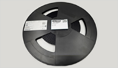
- Step1:Prepare product
-
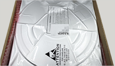
- Step2:Vacuum packaging
-
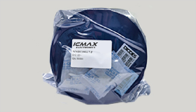
- Step3:Anti-static bag
-
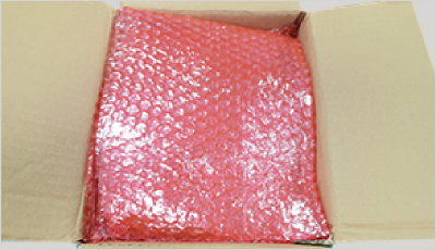
- Step4:Individual package
-
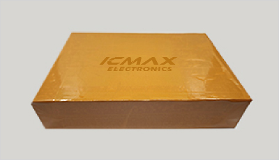
- Step5:Packaging box
-
- Step6:Barcode shipping label
Shipping starts at $40, but some countries will exceed $40. For example (South Africa, Brazil, India, Pakistan, Israel, etc.)
The basic freight (for package ≤0.5kg or corresponding volume) depends on the time zone and country.
Currently, our products are shipped through DHL, FedEx, SF, and UPS.
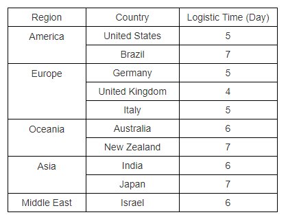
Delivery TimeOnce the goods are shipped, estimated delivery time depends on the shipping methods you chose:
FedEx International, 5-7 business days.
The following are some common countries' logistic time.
- Hot Sale
- Related Categories
- Include Parts
- Popular Search
The following parts include "UT3N06G‑AB3‑R" in Silicon Labs UT3N06G‑AB3‑R.
- Part Number
- Manufacturer
- Package
- Description
- BSZ180P03NS3EGATMA1 Infineon Technologies UT3N06G-AB3-R – UTC N-Channel 60V 3A Enhancement Mode Power MOSFET Quick Answer The UT3N06G-AB3-R is an N-channel enhancement mode power MOSFET from Unisonic Technologies (UTC).
- SIRA14DP-T1-GE3 Vishay Siliconix UT3N06G-AB3-R – UTC N-Channel 60V 3A Enhancement Mode Power MOSFET Quick Answer The UT3N06G-AB3-R is an N-channel enhancement mode power MOSFET from Unisonic Technologies (UTC).
- AO4419 Alpha & Omega Semiconductor Inc. UT3N06G-AB3-R – UTC N-Channel 60V 3A Enhancement Mode Power MOSFET Quick Answer The UT3N06G-AB3-R is an N-channel enhancement mode power MOSFET from Unisonic Technologies (UTC).
- SISA14BDN-T1-GE3 Vishay Siliconix UT3N06G-AB3-R – UTC N-Channel 60V 3A Enhancement Mode Power MOSFET Quick Answer The UT3N06G-AB3-R is an N-channel enhancement mode power MOSFET from Unisonic Technologies (UTC).
- PSMN9R5-30YLC,115 Nexperia USA Inc. UT3N06G-AB3-R – UTC N-Channel 60V 3A Enhancement Mode Power MOSFET Quick Answer The UT3N06G-AB3-R is an N-channel enhancement mode power MOSFET from Unisonic Technologies (UTC).
- BUK9Y21-40E,115 Nexperia USA Inc. UT3N06G-AB3-R – UTC N-Channel 60V 3A Enhancement Mode Power MOSFET Quick Answer The UT3N06G-AB3-R is an N-channel enhancement mode power MOSFET from Unisonic Technologies (UTC).
- RTQ035N03HZGTR Rohm Semiconductor UT3N06G-AB3-R – UTC N-Channel 60V 3A Enhancement Mode Power MOSFET Quick Answer The UT3N06G-AB3-R is an N-channel enhancement mode power MOSFET from Unisonic Technologies (UTC).
- FDMS7680 onsemi UT3N06G-AB3-R – UTC N-Channel 60V 3A Enhancement Mode Power MOSFET Quick Answer The UT3N06G-AB3-R is an N-channel enhancement mode power MOSFET from Unisonic Technologies (UTC).
- RQ3E180BNTB Rohm Semiconductor UT3N06G-AB3-R – UTC N-Channel 60V 3A Enhancement Mode Power MOSFET Quick Answer The UT3N06G-AB3-R is an N-channel enhancement mode power MOSFET from Unisonic Technologies (UTC).
- STL6N2VH5 STMicroelectronics UT3N06G-AB3-R – UTC N-Channel 60V 3A Enhancement Mode Power MOSFET Quick Answer The UT3N06G-AB3-R is an N-channel enhancement mode power MOSFET from Unisonic Technologies (UTC).
The following parts are popular search parts in Test and Measurement.
Inventory:50,000
Please send an inquiry. Send us your inquiry, and we will respond immediately.

- 1500+ Daily average RFQ Volume

- 20,000.000 Standard Product Unit

- 1800+ Worldwide Manufacturers

- 15,000+ In-stock Warehouse


