


Power Integrations TNY288DG

- Part No.:
- TNY288DG
- Manufacturer:
- Power Integrations
- Category:
- AC DC Converters, Offline Switches
- Package:
- 8-SOIC (0.154", 3.90mm Width), 7 Leads
- Datasheet:
-
 TNY288DG.pdf
- Description:
- IC OFFLINE SWITCH FLYBACK 8SO
- Quantity:
-
Unit Price:$0
Ext Price:$0
- Payment:
-

- Shipping:
-


TNY288DG Information
- Specifications
- Product Details
- Comparison
- Tags
- Product attributes
- Attribute value
- Manufacturer:
- Power Integrations
- Series:
- TinySwitch®-4
- Package/Case:
- 8-SOIC (0.154", 3.90mm Width), 7 Leads
- Packaging:
- Tube
- Product Status:
- Discontinued at Digi-Key
- Output Isolation:
- Isolated
- Internal Switch(s):
- Yes
- Voltage - Breakdown:
- 725V
- Topology:
- Flyback
- Voltage - Start Up:
- -
- Voltage - Supply (Vcc/Vdd):
- -
- Duty Cycle:
- 67%
- Frequency - Switching:
- 124kHz ~ 140kHz
- Power (Watts):
- 14.5 W
- Fault Protection:
- Current Limiting, Open Loop, Over Temperature, Over Voltage, Short Circuit
- Control Features:
- EN
- Operating Temperature:
- -40°C ~ 150°C (TJ)
- Grade:
- -
- Qualification:
- -
- Supplier Device Package:
- SO-8C
- Mounting Type:
- Surface Mount
- Datasheet:
-
TNY288DG.pdf
TNY288DG — 14.5W Off-Line Switcher with 725V MOSFET (SO-8C)
The TNY288DG is a TinySwitch-4 off-line switcher from Power Integrations — a 725V power MOSFET and an ON/OFF controller in an SO-8C package, rated 14.5W in a sealed adapter and 26W peak from a 230VAC rail.
From what we see in Shenzhen reorder patterns (2025–2026), the TinySwitch-4 line gets specified when a design needs the higher bus de-rating or the tighter overload limit, rather than for the extra package options.
Here's what the part number hides. The same die ships in three packages and gets three different power ratings — 16W in DIP-8C, 14.5W in this SO-8C, and 23W in eSOP-12B.
And Rev. G prints the reason rather than leaving it implied. The thermal resistance is given per package: 70, 100 and 45°C/W junction-to-air. This package is the middle one, and it is the worst of the three.
One more, because it sets the ceiling: there is no TNY289D or TNY290D. Above TNY288, Power Integrations stops offering the SO-8C at all.
What Are the Technical Specifications of TNY288DG?
| Parameter | Value |
|---|---|
| Type | Off-line switcher with integrated 725V power MOSFET (TinySwitch-4) |
| Package | SO-8C (D) — seven leads, pin 3 absent, plus an exposed pad tied to SOURCE |
| Ordering Code | TNY288DG-TL (D = SO-8C, G = RoHS and halogen-free, TL = tape & reel 1000/reel) |
| Breakdown Voltage (BVDSS) | 725V min |
| DRAIN Voltage (abs max) | −0.3V to 725V |
| DRAIN Peak Current (abs max) | 1040mA (1950mA while DRAIN stays below 400V) |
| Output Power, 230VAC ±15% | 14.5W enclosed adapter / 26W open-frame peak |
| Output Power, 85–265VAC | 9W enclosed adapter / 19.5W open-frame peak |
| Standard Current Limit (0.1µF BP/M) | 550mA typ (512 min / 588 max) |
| Reduced Current Limit (1µF BP/M) | 450mA typ (419 min / 499 max) |
| Increased Current Limit (10µF BP/M) | 650mA typ (605 min / 721 max) |
| On-State Resistance, TJ = 25°C | 6.0Ω max (5.2Ω min, ID = 55mA) |
| On-State Resistance, TJ = 100°C | 9.0Ω max (7.8Ω min) |
| Switching Frequency | 132kHz typ (124–140kHz), 8kHz peak-to-peak jitter |
| Maximum Duty Cycle | 67% typ (62% min, S1 open) |
| Line-Compensated Overload Power | Yes — typical OCP change from 85VAC to 265VAC is under 15% |
| Thermal Shutdown Temperature | 142°C typ (135 min / 150 max), 75°C hysteresis |
| Auto-Restart ON-Time | 64ms typ; auto-restart duty cycle 3% typ |
| OFF-State Drain Leakage | 100µA max at 125°C, VDS = 560V |
| DRAIN Supply Current | 615µA typ / 650µA max (EN/UV open, switching) |
| BP/M Shutdown Threshold Current | 6.5mA typ (4 min / 9 max) |
| BP/M Power-Up Reset Voltage | 3.0V typ (1.6 min / 3.6 max) |
| Thermal Resistance (θJA), D package | 100°C/W on 232mm² copper; 80°C/W on 645mm² copper |
| Thermal Resistance (θJC), D package | 30°C/W (case measured at the bottom-side exposed pad) |
| Operating Junction Temperature | −40°C to 150°C |
| No-Load Consumption | <150mW at 265VAC without bias winding; <30mW with |
Two rows here are not like the TinySwitch-III sheet, and both are additions rather than changes. The first is line-compensated overload power, which holds the over-current trip point steady across the input range.
The second is package-specific thermal resistance. Rev. N of the TinySwitch-III sheet prints one figure covering both of its packages. Rev. G of this one prints three.
Why Does the Same Die Have Three Different Power Ratings?
Because the thermal path differs, and TinySwitch-4 publishes it per package. Here is the junction-to-air figure for the TNY288 die in each of its three packages, on the same copper area.
Lower is better, and the SO-8C is 43% worse than the DIP-8C. The junction-to-case figure tells the same story: 11°C/W for the DIP, 30°C/W for the SO-8C, and 2°C/W for the eSOP-12B.
The eSOP-12B manages 45°C/W because its exposed pad is large and solders straight to the board. The SO-8C also has an exposed pad, but a far smaller one — the die is the same and the escape path is not.
The three lines start together and split as the family grows. At TNY284 the packages are interchangeable on paper; by TNY288 the eSOP-12B carries 59% more than the SO-8C. Then the SO-8C line simply stops.
That is the useful form of this chart: the package only becomes a design decision once you are above roughly 12W.
What Is Line-Compensated Overload Power?
It holds the over-current trip point steady as the input voltage moves. On TinySwitch-III the typical overload power changes by more than 40% between 85VAC and 265VAC. On TinySwitch-4 that change is under 15%, with no additional components.
The practical effect lands on the transformer and the clamp. Whatever the part delivers during a fault has to be absorbed somewhere, so an uncompensated design must be built for the worst-case line. Compensation narrows that band and lets the magnetics be sized for a smaller number.
The exposed pad is not optional. It is internally tied to SOURCE, so it is part of the circuit, and it is also the shortest thermal path this package has — the 30°C/W junction-to-case figure is measured there.
Build the footprint for seven leads plus the pad. A library part copied from a generic SOIC-8 template will place a pad where pin 3 should be, and omit the one pad that matters.
When Should You Use (and NOT Use) the TNY288DG?
✅ Use TNY288DG when:
- You need up to 14.5W enclosed from a universal input, or 9W on the 85–265VAC row. Those are the two ratings that apply to this package, and they are lower than the DIP version's.
- Your board is reflow-assembled and space is tight. The SO-8C is the smallest of the three TNY288 packages — that is what you are buying, and the power rating is what it costs.
- You want the tighter overload band. Line-compensated OCP keeps the trip point within 15% across the input range instead of over 40%.
- Your reflected voltage is high. The 725V rating gives more headroom than the 700V TinySwitch-III parts at the same bus voltage.
- You are migrating from a pin-compatible TinySwitch-III design. Same pinout, same BP/M current-limit scheme, same ON/OFF control architecture.
❌ Don't use TNY288DG when:
- You need more than about 15W enclosed. The DIP-8C version gives 16W and the eSOP-12B gives 23W from the same die. If you have the board area, this package is the wrong one.
- You have no copper to give it. At 100°C/W on a small pour, the usable power falls well below the table. The rating assumes a real thermal pad.
- You need TNY289 or TNY290 power. Neither has a D variant. The SO-8C line ends here.
- You cannot reflow. The exposed pad needs a stencil and a reflow profile; there is no through-hole option in this package.
- You are replacing a TNY288P without checking the rating. Pin-compatible does not mean power-compatible — you would be dropping from 16W to 14.5W.
What Are the Alternatives to TNY288DG?
| Model | Type | Key Difference | Best For |
|---|---|---|---|
| TNY288PG | TinySwitch-4, DIP-8C | Same die, 16W adapter / 28W peak; θJA 70°C/W. Needs a through-hole step | Boards with room, or hand-assembled runs |
| TNY288KG | TinySwitch-4, eSOP-12B | Same die, 23W adapter / 28W peak; θJA 45°C/W. Larger footprint, largest thermal pad | Anything above 15W that needs to stay surface-mount |
| TNY287DG | TinySwitch-4, SO-8C | One family step down: 11.5W / 23.5W, same package and pad | Designs already comfortable below 11W |
| TNY279GN | TinySwitch-III, SMD-8C | 700V instead of 725V, no line-compensated OCP; 18W / 32W and no exposed pad | Pin-compatible fallback where the older generation is already qualified |
Here's the thing worth noticing about that table: all four parts are pin-compatible and the current limits overlap heavily. Moving between them is a board-layout decision, not a circuit redesign.
The TNY288DG's standard 550mA equals the TNY279GN's increased setting. Its reduced 450mA equals the TNY278GN's standard setting. The families line up on purpose.
What does not line up is the thermal budget. Dropping this part onto a footprint designed for the DIP version moves you from 70°C/W to 100°C/W at the same power — about a 30°C hotter junction for every watt dissipated.
What Are the Typical Applications of TNY288DG?
PC standby and auxiliary supplies. Power Integrations names these directly, and they are where line-compensated OCP earns its place: an unusually high load current in a standby rail usually means a fault, and the tighter trip band limits how much power can be delivered into it.
Appliance and metering supplies. The 725V rating covers high reflected-voltage designs that would eat too far into a 700V part's margin, and the thermal shutdown with automatic recovery suits equipment that must come back without a service call.
Adapters where the enclosure is small. The SO-8C is the compact option of the three packages. Sizing the design to 14.5W or below is what buys the small footprint; the copper under the exposed pad is what makes it real.
Surface-mount migration of existing TinySwitch designs. Same pinout and same BP/M scheme mean a board respin rather than a circuit change — with the power row re-checked for the package you moved to.
Why Buy TNY288DG from ICMASS?
We test incoming TinySwitch-4 lots against the rows that decide whether the package survives: the current limit at each BP/M capacitor value, and the on-state resistance. On a remarked part those numbers drift first.
We stock the TNY288 die in more than one package — SO-8C, DIP-8C and eSOP-12B — alongside the TinySwitch-III SMD line. If the thermal calculation says this package is too small, the answer is a stock question rather than a new supplier.
Send us the output power, the worst-case line voltage and the copper area under the pad and we will tell you which package the numbers actually support. That is frequently not the one currently on the board.
Orders ship same day from Shenzhen, and the official Power Integrations PDF for every part we quote travels with the quote.
Frequently Asked Questions About TNY288DG
Q1: Can I replace a TinySwitch-III part with a TinySwitch-4 part?
A: Yes — they are pin-compatible, and the current-limit scheme is the same. Rev. G states the intent explicitly. You gain the 725V rating, line-compensated overload power and a tighter undervoltage threshold. What you must re-check is the package: TinySwitch-III's SMD-8C and TinySwitch-4's SO-8C are different parts with different footprints.
Q2: Why is the SO-8C version rated lower than the DIP version?
A: Because its thermal path is worse, and Rev. G prints the figure. The TNY288 die is specified at 70°C/W in the DIP-8C, 100°C/W in the SO-8C and 45°C/W in the eSOP-12B. The power rows follow: 16W, 14.5W and 23W. Same die, three ratings, one reason.
Q3: What does the exposed pad connect to?
A: SOURCE, internally. Figure 4 of the datasheet states it directly. That makes the pad part of the circuit as well as the thermal path, and it is where the 30°C/W junction-to-case figure is measured. Solder it with vias into an inner plane; leaving it unconnected gives away most of this package's dissipation capability.
Q4: Is there a TNY289DG or TNY290DG?
A: No. The TinySwitch-4 output power table lists TNY289P and TNY289K, and TNY290P and TNY290K — there is no D variant for either. The SO-8C is offered up to TNY288 and no further, which puts its practical ceiling at 14.5W enclosed.
Q5: What is line-compensated overload power actually for?
A: It keeps the over-current trip point from drifting with input voltage. TinySwitch-III's typical OCP changes by more than 40% between 85VAC and 265VAC; TinySwitch-4 holds it under 15%. The benefit is in the magnetics: an uncompensated design must be sized for the worst-case line, so narrowing the band lets the transformer and clamp be built around a smaller number.
Q6: Why would I choose 725V over 700V?
A: For de-rating headroom on high reflected-voltage designs. The drain sees the reflected output voltage plus the leakage-inductance spike on top of the bus. Power Integrations lists the increased breakdown margin as a headline feature, and it matters most where the turns ratio is high or the clamp is deliberately loose.
Q7: My board ran a TNY287DG and the current limit stayed low after a load step. Is that normal?
A: There is a reported case of exactly that on Power Integrations' forum, with about 20°C of extra temperature rise. The state machine is meant to restore the higher limit at heavy load. If you see the limit stay reduced after a high-to-low-to-high load step, scope the DRAIN current rather than the voltage, and confirm the EN/UV sampling is behaving.
Q8: How much copper does the SO-8C pad need?
A: 232mm² gives 100°C/W; 645mm² gives 80°C/W. Those are the only two board-level figures Rev. G publishes for this package, and both assume the pad is soldered to that area. Below 232mm² you are outside the specified range and the power table no longer describes your board.
Q9: What is the difference between SMD-8C and SO-8C?
A: They are different packages from different generations. SMD-8C (G) is the TinySwitch-III surface-mount package and has no exposed pad. SO-8C (D) is a TinySwitch-4 addition, and it does have one, tied to SOURCE. They are not footprint-compatible, so a migration between generations needs a layout change.
Q10: Can I get no-load consumption below 50mW?
A: Yes, and TinySwitch-4 improves the number. Self-powered from the DRAIN pin the part draws under 150mW at 265VAC. Add a bias winding feeding the BP/M pin with at least 1mA and the datasheet figure drops below 30mW — better than the TinySwitch-III equivalent, which specifies under 50mW.
| Image |

|
|
| Part Number | TNY288DG-TL | TNY288DG |
| Manufacturer | Power Integrations | Power Integrations |
| Series | TinySwitch®-4 | TinySwitch®-4 |
| Package/Case | 8-SOIC (0.154", 3.90mm Width), 7 Leads | 8-SOIC (0.154", 3.90mm Width), 7 Leads |
| Packaging | Tape & Reel (TR) | Tube |
| Product Status | Active | Discontinued at Digi-Key |
| Output Isolation | Isolated | Isolated |
| Internal Switch(s) | Yes | Yes |
| Voltage - Breakdown | 725V | 725V |
| Topology | Flyback | Flyback |
| Voltage - Start Up | - | - |
| Voltage - Supply (Vcc/Vdd) | - | - |
| Duty Cycle | 67% | 67% |
| Frequency - Switching | 124kHz ~ 140kHz | 124kHz ~ 140kHz |
| Power (Watts) | 14.5 W | 14.5 W |
| Fault Protection | Current Limiting, Open Loop, Over Temperature, Over Voltage, Short Circuit | Current Limiting, Open Loop, Over Temperature, Over Voltage, Short Circuit |
| Control Features | EN | EN |
| Operating Temperature | -40°C ~ 150°C (TJ) | -40°C ~ 150°C (TJ) |
| Grade | - | - |
| Qualification | - | - |
| Supplier Device Package | SO-8C | SO-8C |
| Mounting Type | Surface Mount | Surface Mount |
User Guide
- Purchase & Inquiry
- Package
- Shipping Information
- Customer Review
You may place an order without registering to IC-MAX.COM
We strongly suggest you sign in before purchasing as you can track your order in real time.
For your convenience, we accept multiple payment methods in USD, including PayPal, Credit Card, and wire transfer.
RFQ (Request for Quotations)
It is recommended to request for quotations to get the latest prices and inventories about the part.
Our sales will reply to your request by email within 24 hours.
1. You'll receive an order information email in your inbox. (Please remember to check the spam folder if you didn't hear from us).
2. Since inventories and prices may fluctuate to some extent, the sales manager is going to reconfirm the order and let you know if there are any updates.
-
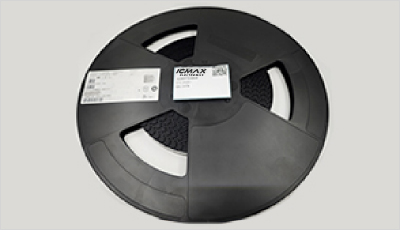
- Step1:Prepare product
-
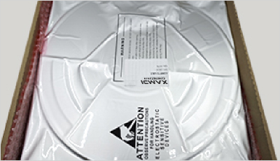
- Step2:Vacuum packaging
-
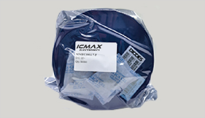
- Step3:Anti-static bag
-
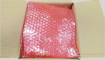
- Step4:Individual package
-
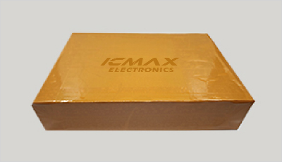
- Step5:Packaging box
-
- Step6:Barcode shipping label
Shipping starts at $40, but some countries will exceed $40. For example (South Africa, Brazil, India, Pakistan, Israel, etc.)
The basic freight (for package ≤0.5kg or corresponding volume) depends on the time zone and country.
Currently, our products are shipped through DHL, FedEx, SF, and UPS.
Delivery TimeOnce the goods are shipped, estimated delivery time depends on the shipping methods you chose:
FedEx International, 5-7 business days.
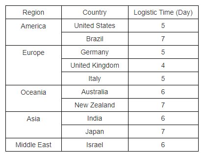
The following are some common countries' logistic time.
- Hot Sale
- Related Categories
- Include Parts
- Popular Search
- Voltage Regulators - Linear, Low Drop Out (LDO) Regulators(66836)
- Voltage Regulators - Linear Regulator Controllers(325)
- Voltage Regulators - Linear + Switching(1473)
- Voltage Regulators - DC DC Switching Regulators(35756)
- Voltage Reference(8428)
- V/F and F/V Converters(139)
- Thermal Management(515)
- Supervisors(41287)
- Special Purpose Regulators(4820)
- RMS to DC Converters(144)
The following parts include "TNY288DG" in Silicon Labs TNY288DG.
- Part Number
- Manufacturer
- Package
- Description
- LNK6407D-TL Power Integrations 8-SOIC (0.154", 3.90mm Width), 7 Leads IC OFFLINE SWITCH FLYBACK 8SO
- LNK3204D-TL Power Integrations 8-SOIC (0.154", 3.90mm Width), 7 Leads IC OFFLINE SWITCH FLYBACK 8SO
- SR10LG-G Microchip Technology 8-SOIC (0.154", 3.90mm Width), 7 Leads IC OFFLINE SWITCH FLYBACK 8SO
- TNY285DG-TL Power Integrations 8-SOIC (0.154", 3.90mm Width), 7 Leads IC OFFLINE SWITCH FLYBACK 8SO
- LNK304DN-TL Datasheet, Price, Stock & Alternatives | ICMASS Power Integrations 8-SOIC (0.154", 3.90mm Width), 7 Leads IC OFFLINE SWITCH FLYBACK 8SO
- TNY285KG-TL Power Integrations 8-SOIC (0.154", 3.90mm Width), 7 Leads IC OFFLINE SWITCH FLYBACK 8SO
- LNK3206D-TL Power Integrations 8-SOIC (0.154", 3.90mm Width), 7 Leads IC OFFLINE SWITCH FLYBACK 8SO
- LNK623DG-TL Power Integrations 8-SOIC (0.154", 3.90mm Width), 7 Leads IC OFFLINE SWITCH FLYBACK 8SO
- TNY286PG Power Integrations 8-SOIC (0.154", 3.90mm Width), 7 Leads IC OFFLINE SWITCH FLYBACK 8SO
- LNK624DG-TL Power Integrations 8-SOIC (0.154", 3.90mm Width), 7 Leads IC OFFLINE SWITCH FLYBACK 8SO
The following parts are popular search parts in Test and Measurement.
Inventory:0
Please send an inquiry. Send us your inquiry, and we will respond immediately.

- 1500+ Daily average RFQ Volume

- 20,000.000 Standard Product Unit

- 1800+ Worldwide Manufacturers

- 15,000+ In-stock Warehouse


