


Power Integrations LNK3206D-TL

- Part No.:
- LNK3206D-TL
- Manufacturer:
- Power Integrations
- Category:
- AC DC Converters, Offline Switches
- Package:
- 8-SOIC (0.154", 3.90mm Width), 7 Leads
- Datasheet:
-
 LNK3206D-TL.pdf
- Description:
- IC OFFLINE SWITCH MULT TOP 8SO
- Quantity:
-
Unit Price:$0.910000
Ext Price:$0.910000
- Payment:
-

- Shipping:
-


LNK3206D-TL Information
- Specifications
- Product Details
- Comparison
- Tags
- Product attributes
- Attribute value
- Manufacturer:
- Power Integrations
- Series:
- LinkSwitch™-TN2
- Package/Case:
- 8-SOIC (0.154", 3.90mm Width), 7 Leads
- Packaging:
- Tape & Reel (TR)
- Product Status:
- Active
- Output Isolation:
- Non-Isolated
- Internal Switch(s):
- Yes
- Voltage - Breakdown:
- 725V
- Topology:
- Buck, Buck-Boost, Flyback
- Voltage - Start Up:
- -
- Voltage - Supply (Vcc/Vdd):
- -
- Duty Cycle:
- 69%
- Frequency - Switching:
- 66kHz
- Power (Watts):
- -
- Fault Protection:
- Current Limiting, Over Temperature, Over Voltage, Short Circuit
- Control Features:
- -
- Operating Temperature:
- -40°C ~ 125°C (TJ)
- Grade:
- -
- Qualification:
- -
- Supplier Device Package:
- SO-8C
- Mounting Type:
- Surface Mount
- Datasheet:
-
LNK3206D-TL.pdf
LNK3206D-TL — 360mA Non-Isolated Buck Switcher, LinkSwitch-TN2 (SO-8C)
The LNK3206D-TL is the highest-current member of Power Integrations' LinkSwitch-TN2 family — a non-isolated offline switcher that delivers 225mA in MDCM / 360mA in CCM from universal AC input. Its core numbers: 725V MOSFET, 66kHz fixed switching with frequency jittering, and <30mW no-load with external bias.
In Shenzhen distribution, the LNK3206 moves in high volume to appliance and smart meter manufacturers. It's the part engineers pick when they need a small, cheap offline supply and don't need a transformer.
LinkSwitch-TN2 is the IC that replaces cap-dropper and linear regulator designs — same simplicity, an order of magnitude less wasted power. The LNK3206 is the top of the family, for when you need the most current the SO-8C package can deliver.
What Are the Technical Specifications of LNK3206D-TL?
| Parameter | Value |
|---|---|
| Manufacturer | Power Integrations |
| Series | LinkSwitch™-TN2 (LNK3202–LNK3207) |
| Topology | Non-isolated Buck (Buck-Boost and Flyback also supported) |
| Integrated Switch | 725V Power MOSFET |
| Switching Frequency | 66kHz fixed, with ±4kHz frequency jittering for EMI |
| Duty Cycle | 69% max |
| Output Current (MDCM) | 225mA (85–265VAC or 230VAC) |
| Output Current (CCM) | 360mA (85–265VAC or 230VAC, with larger inductor + ultrafast diode) |
| Current Limit (default) | 482mA typ (BP pin cap = 0.1µF) |
| Current Limit (reduced) | 370mA typ (BP pin cap = 1µF) |
| Drain Peak Current | 3,750mA (scaling factor 6.25 vs 2.05 for LNK3204) |
| No-Load Consumption | <30mW with external bias; <50mW without |
| Standby Supply Current | <100µA |
| Control Method | ON/OFF control — constant efficiency across load range |
| Input Voltage (AC) | 85VAC – 265VAC (full universal range) |
| Fault Protection | Current limiting, output OVP, line input OVP (OVL), hysteretic thermal shutdown (142°C), short-circuit auto-restart (<3% max power during fault) |
| Current Limit Selection | Via BP pin capacitor: 0.1µF = standard (482mA) / 1µF = reduced (370mA) |
| Package | SO-8C (7-lead, 3.90mm body width, extended creepage between DRAIN and other pins) |
| Operating Temperature | -40°C to +125°C (TJ) |
Per the Power Integrations LinkSwitch-TN2 datasheet (Rev B, LNK3202-3207).
What "non-isolated buck" means in practice: the LNK3206 rectifies AC to DC, then bucks it down with a single inductor and a freewheeling diode. No transformer. No optocoupler. The feedback comes through a resistor divider directly from the output.
The 725V MOSFET matters because rectified 265VAC peaks at ~375V. On a bad day with line surges, you'll kiss 500V+. The 725V rating gives you margin that a 600V or 650V part wouldn't.
When Should You Use (and NOT Use) the LNK3206D-TL?
✅ Use LNK3206D-TL when:
- You need 100–360mA from AC mains with the lowest possible BOM. One IC, one inductor, one freewheeling diode, two capacitors, and a handful of resistors. That's the entire non-isolated buck BOM. Compared to a TinySwitch flyback (transformer + optocoupler + TL431), you're cutting the BOM cost by 30–50%.
- Galvanic isolation is not a safety requirement. Smart meters, LED bulb drivers, appliance control boards, IoT sensor nodes, and HVAC thermostats all have the entire circuit enclosed and user-inaccessible. In these applications, isolation adds cost with no safety benefit.
- Standby power is your primary constraint. At <30mW no-load with external bias, the LNK3206 sails under every global standby regulation. Cap-dropper supplies burn 0.5–2W doing nothing. A linear regulator at 100mA from 12V dumps 2–3W in heat. The LNK3206 replaces both with a single chip.
- You're retrofitting a cap-dropper or linear supply. The LNK3206 fits in roughly the same PCB area as a cap-dropper but runs cool, handles input surges gracefully, and delivers regulated output across the full AC range.
❌ Don't use LNK3206D-TL when:
- You need galvanic isolation. If the output is user-accessible (USB charger, appliance panel), you need a safety isolation barrier. Use TNY280 (TinySwitch-III) or LNK625 (LinkSwitch-CV) for isolated flyback designs instead.
- You need more than 360mA. The LNK3206 is the current ceiling of LinkSwitch-TN2 in the SO-8C package. At 360mA CCM, the inductor must handle the full 482mA peak without saturating. For higher currents, move up to the LNK3207 in a larger package or switch to a flyback with TinySwitch.
- Your output voltage is close to the rectified DC bus. A buck converter can only step down. If you need 200VDC from a 230VAC rectified bus (~325VDC), a non-isolated buck works. But if you need 12V from a 12VAC input after rectification, the dropout voltage leaves no headroom.
- You need precision regulation better than ±3%. The LNK3206 regulates via the FEEDBACK pin and a resistor divider. Regulation is typically ±3–5% over line and load. For tighter specs, add a TL431 as a secondary reference on the feedback path.
LNK3204 vs LNK3205 vs LNK3206 — Which LinkSwitch-TN2 Fits?
The LinkSwitch-TN2 family scales from 120mA to 360mA (buck, MDCM). Same architecture, same SO-8C package, different MOSFET die sizes.
CCM vs MDCM: CCM (continuous conduction mode) doubles the output current but requires a larger inductor and an ultrafast freewheeling diode (tRR ≤ 35ns). For most appliance and IoT applications at 12V/150mA, MDCM with a cheap SMD inductor is the right call.
One thing engineers miss: the LNK3206's drain peak current is 3,750mA — over 3× the LNK3204. This matters for startup into a discharged output capacitor and for surviving line surges.
Pin Functions at a Glance
| Pin | Name | Function |
|---|---|---|
| 1 | FEEDBACK (FB) | Output voltage sense input. Connect to the output via a resistor divider. The IC regulates by comparing the FB pin voltage to an internal 1.65V reference. When the FB pin current exceeds 670µA, output OVP triggers and the IC enters auto-restart. Keep this trace away from the DRAIN trace — it's a high-impedance node. |
| 2 | BYPASS (BP) | Internal 5.2V regulator bypass and current limit selector. Connect 0.1µF to SOURCE for standard current limit (482mA) or 1µF for reduced current limit (370mA). These are the only two recommended values — intermediate values cause erratic operation. Do not use 1nF or 10nF. |
| 3,4 | SOURCE (S) | MOSFET source return and IC ground reference. Connect to the ground plane with short, wide traces. The SOURCE pins are the primary thermal path — at 360mA CCM, copper area on SOURCE matters for junction temperature. |
| 5,6,7 | DRAIN (D) | 725V MOSFET drain. Connect to the buck inductor and the input DC bus through the inductor. Pin 7 (the rightmost DRAIN pin) has extended creepage distance from other pins for high-voltage reliability. The DRAIN copper area also serves as a heatsink — don't minimize it unnecessarily. |
| — | (No pin 8) | Intentionally omitted. The missing pin extends the creepage distance between the high-voltage DRAIN node and the low-voltage control pins, improving reliability in humid or polluted environments. |
What Are the Typical Applications of LNK3206D-TL?
Smart meter power supply (3.3V or 5V at 150–250mA). This is the LNK3206's bread and butter. A smart meter needs a tiny always-on supply from AC mains for the MCU, RF module, and display.
The LNK3206 + a 1mH SMD inductor + a 100µF output cap delivers regulated 5V from 85–265VAC in less than 15 × 20mm of PCB.
LED bulb / smart LED driver (12–48V at 100–200mA). Non-isolated LED drivers in fully enclosed bulbs don't need a transformer. The LNK3206 in a buck topology drives a string of LEDs directly from rectified AC with an output voltage set by the LED string and a sense resistor.
Home automation / IoT sensor node (3.3V at 50–150mA). Wi-Fi or Zigbee sensors that plug into mains need microamps of standby current. The LNK3206 with external bias draws <100µA in standby before the sensor wakes up.
Appliance control board auxiliary rail (12V or 24V at 100–200mA). Washing machines, refrigerators, and HVAC controllers need low-voltage rails for relays, MCUs, and sensors. The LNK3206 generates these from the AC input with fewer components than a flyback.
What Are the Alternatives to LNK3206D-TL?
| Model | Family | Key Difference | Best For |
|---|---|---|---|
| LNK3205D-TL | LinkSwitch-TN2 | 270mA CCM, 375mA ILIM, same SO-8C pinout | When 360mA is overkill — smaller inductor, lower cost |
| LNK3204D-TL | LinkSwitch-TN2 | 170mA CCM, 257mA ILIM, lowest cost in family | Sub-150mA designs where every cent counts |
| LNK3207D-TL | LinkSwitch-TN2 | Highest TN2 current, larger package option | When the LNK3206 maxes out — 400mA+ buck designs |
| TNY284DG-TL | TinySwitch-4 | 725V, isolated flyback, 8.5W, selectable ILIM | When you need galvanic isolation at similar cost |
| LNK625DG-TL | LinkSwitch-CV | 725V, isolated flyback, 6.5W, primary-side CV regulation | Isolated low-power where output regulation matters |
LNK3206 vs TNY284 — non-isolated buck vs isolated flyback. The LNK3206 gives you a buck converter: one inductor, one diode, five passives. The TNY284 gives you an isolated flyback: transformer, optocoupler, TL431, RCD clamp.
The LNK3206 wins on BOM cost and PCB area. The TNY284 wins when the output is user-touchable and safety isolation is mandatory.
LNK3206 vs LNK625 — two different non-isolated needs. The LNK625 is an isolated flyback switcher with primary-side regulation. It's for when you need precise CV regulation but don't want the full optocoupler feedback chain.
Per the LinkSwitch-TN2 datasheet (Rev B), the LNK3206's default current limit of 482mA gives roughly 3× the output current of a comparable LNK3204.
How Much Does the LNK3206D-TL Cost and Is It in Stock?
| Quantity | Reference Price (per unit) |
|---|---|
| 1–99 | $0.85–$1.20 |
| 100–999 | $0.55–$0.80 |
| 1,000–2,499 | $0.45–$0.60 |
| 2,500+ (full reel) | $0.38–$0.50 |
Contact ICMASS for a same-day quote. The LNK3206D-TL is an active production part with broad availability. SO-8C tape & reel ships in 2,500-unit increments.
At volume, the LNK3206 is one of the lowest-cost ways to get a regulated DC rail from AC mains — typically 40–60% cheaper than a comparable isolated flyback when you factor in the saved transformer, optocoupler, and TL431.
Why Buy LNK3206D-TL from ICMASS?
Complete LinkSwitch-TN2 lineup in stock. We carry LNK3202 through LNK3207 across SO-8C (D), SMD-8C (G), and PDIP-8C (P) packages. If your first design uses a LNK3204 and your next product needs the LNK3206, we have both.
Inductor selection and layout review. The #1 support issue we see with LNK3206 designs: inductor saturation. The 482mA current limit means your inductor must handle the full peak without saturating at the maximum junction temperature.
Tell us your output voltage and target current. We'll recommend an inductor that works at 66kHz with enough saturation margin, and flag the layout issues that trip up first-time LinkSwitch-TN2 designs.
One-stop BOM for non-isolated buck supplies. A complete LNK3206 buck design needs the IC, a power inductor, a freewheeling diode, input/output capacitors, and FB divider resistors. We stock every part in the standard reference design. One PO covers the entire supply.
Shenzhen warehouse, global shipping. Orders before 15:00 CST ship same day. DHL/FedEx delivery in 5–10 days.
Frequently Asked Questions About LNK3206D-TL
Q1: Why does the LNK3206 have two current limits and which one should I use?
A: The BP pin capacitor sets the current limit: 0.1µF = 482mA standard, 1µF = 370mA reduced. Use standard limit (0.1µF) when you need maximum output current — up to 360mA in CCM. Use reduced limit (1µF) when output current is <200mA and you want to use a smaller, cheaper SMD inductor.
These are the only two recommended values. Don't use intermediate values like 500nF — the IC's internal detection circuit expects one or the other, and intermediate capacitance causes erratic current limit behavior.
Q2: My LNK3206 enters auto-restart at startup — what's wrong?
A: Three common causes, check them in this order. First, the BP capacitor value: verify it's exactly 0.1µF or 1µF. A 1nF cap causes immediate malfunction. Second, the output capacitor may be too large: >100µF prevents the output from reaching regulation within the 50ms auto-restart window.
Third, output OVP tripping: if the FB pin current exceeds 670µA (typically from output overshoot at startup), the IC interprets this as an overvoltage fault. Add a small resistor in series with the optocoupler transistor or a 1–3mA preload on the output to clamp the startup overshoot.
Q3: Why am I getting 34V on the output instead of 5V?
A: The FB resistor divider is off, or the feedback diode forward voltage isn't accounted for. The LNK3206 regulates the FB pin to 1.65V. If the upper divider resistor is too high, the output voltage will run away before the FB pin sees 1.65V.
The freewheeling diode and the feedback diode should ideally have the same VF for good regulation. If they're mismatched, adjust the upper FB resistor to compensate. Follow the PI Expert values, not the application note schematic values — PI Expert accounts for your specific diode selections.
Q4: How do I reduce output ripple on my LNK3206 buck?
A: The three things that make the biggest difference. One: use a low-ESR (or very-low-ESR) output capacitor — ceramic is best, keep total capacitance ≤100µF. Two: PCB layout. Keep the FB trace far away from the DRAIN trace, minimize the switch-node copper area, and make the SW-Drain-input-cap loop as small as possible.
Three: use a proper oscilloscope ripple probe for measurement. The ground clip on a standard probe picks up the switching node's magnetic field and shows fake ripple that isn't actually on the output. Spring-clip probe or direct coaxial connection only.
Q5: Can I use the LNK3206 for a 3.3V output?
A: Yes, but the feedback divider resistors need adjustment. The internal FB reference is 1.65V. For a 3.3V output, the upper/lower divider ratio is (3.3 / 1.65) − 1 = 1, so use equal-value resistors (e.g., 10kΩ + 10kΩ).
At 3.3V output, the freewheeling diode's VF (typically 0.5–1V) becomes a significant fraction of the output — use a Schottky diode and account for VF in the divider. Also, the minimum preload of 3mA must be maintained or regulation will be poor at light load.
Q6: What's the difference between LNK3206D, LNK3206G, and LNK3206P?
A: Package only, same die. D = SO-8C (7-lead SMD, narrow body, 3.90mm, lowest cost). G = SMD-8C (7-lead SMD, gull-wing, slightly better thermals). P = PDIP-8C (7-lead through-hole, best thermals, easiest to hand-solder).
The D package is the go-to for automated assembly. The P package is preferred for prototyping and low-volume production where hand-soldering is used.
Q7: My LNK3206 design works fine at 230VAC but fails at 85VAC — why?
A: The inductor saturates at low line. At 85VAC, the rectified DC bus is ~120VDC. To deliver the same output power, the peak inductor current is nearly 2× what it is at 230VAC. If the inductor's saturation current (ISAT) is marginal at 230VAC, it'll saturate hard at 85VAC.
The fix: verify the inductor's ISAT rating at the IC's maximum current limit (482mA for standard, 370mA for reduced) plus at least 20% margin. Don't rely on the inductor's nominal inductance at 0A — inductance drops as current rises.
Q8: Is there an LTspice model for the LNK3206?
A: No — Power Integrations doesn't provide LTspice models for LinkSwitch-TN2. Design must be done through PI Expert Online (piexpertonline.power.com) for automated calculations, and verified on the bench. AN-70 (LinkSwitch-TN2 Design Guide) has the complete design equations if you prefer to calculate by hand. Start with the reference design DER-507 for a 5V buck and adapt component values.
| Image |

|
| Part Number | LNK3206D-TL |
| Manufacturer | Power Integrations |
| Series | LinkSwitch™-TN2 |
| Package/Case | 8-SOIC (0.154", 3.90mm Width), 7 Leads |
| Packaging | Tape & Reel (TR) |
| Product Status | Active |
| Output Isolation | Non-Isolated |
| Internal Switch(s) | Yes |
| Voltage - Breakdown | 725V |
| Topology | Buck, Buck-Boost, Flyback |
| Voltage - Start Up | - |
| Voltage - Supply (Vcc/Vdd) | - |
| Duty Cycle | 69% |
| Frequency - Switching | 66kHz |
| Power (Watts) | - |
| Fault Protection | Current Limiting, Over Temperature, Over Voltage, Short Circuit |
| Control Features | - |
| Operating Temperature | -40°C ~ 125°C (TJ) |
| Grade | - |
| Qualification | - |
| Supplier Device Package | SO-8C |
| Mounting Type | Surface Mount |
User Guide
- Purchase & Inquiry
- Package
- Shipping Information
- Customer Review
You may place an order without registering to IC-MAX.COM
We strongly suggest you sign in before purchasing as you can track your order in real time.
For your convenience, we accept multiple payment methods in USD, including PayPal, Credit Card, and wire transfer.
RFQ (Request for Quotations)
It is recommended to request for quotations to get the latest prices and inventories about the part.
Our sales will reply to your request by email within 24 hours.
1. You'll receive an order information email in your inbox. (Please remember to check the spam folder if you didn't hear from us).
2. Since inventories and prices may fluctuate to some extent, the sales manager is going to reconfirm the order and let you know if there are any updates.
-
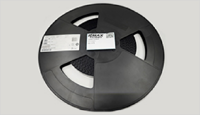
- Step1:Prepare product
-
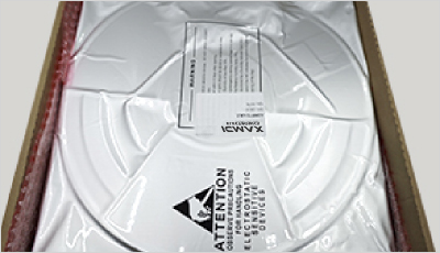
- Step2:Vacuum packaging
-
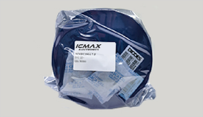
- Step3:Anti-static bag
-
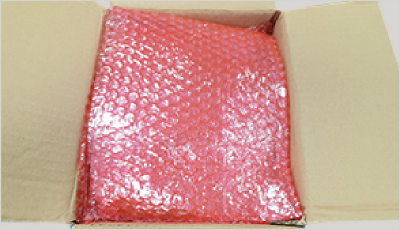
- Step4:Individual package
-
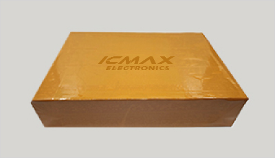
- Step5:Packaging box
-
- Step6:Barcode shipping label
Shipping starts at $40, but some countries will exceed $40. For example (South Africa, Brazil, India, Pakistan, Israel, etc.)
The basic freight (for package ≤0.5kg or corresponding volume) depends on the time zone and country.
Currently, our products are shipped through DHL, FedEx, SF, and UPS.
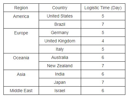
Delivery TimeOnce the goods are shipped, estimated delivery time depends on the shipping methods you chose:
FedEx International, 5-7 business days.
The following are some common countries' logistic time.
- Hot Sale
- Related Categories
- Include Parts
- Popular Search
- Voltage Regulators - Linear, Low Drop Out (LDO) Regulators(66836)
- Voltage Regulators - Linear Regulator Controllers(325)
- Voltage Regulators - Linear + Switching(1473)
- Voltage Regulators - DC DC Switching Regulators(35756)
- Voltage Reference(8428)
- V/F and F/V Converters(139)
- Thermal Management(515)
- Supervisors(41287)
- Special Purpose Regulators(4820)
- RMS to DC Converters(144)
The following parts include "LNK3206D-TL" in Silicon Labs LNK3206D-TL.
- Part Number
- Manufacturer
- Package
- Description
- LNK6407D-TL Power Integrations 8-SOIC (0.154", 3.90mm Width), 7 Leads IC OFFLINE SWITCH MULT TOP 8SO
- LNK3204D-TL Power Integrations 8-SOIC (0.154", 3.90mm Width), 7 Leads IC OFFLINE SWITCH MULT TOP 8SO
- SR10LG-G Microchip Technology 8-SOIC (0.154", 3.90mm Width), 7 Leads IC OFFLINE SWITCH MULT TOP 8SO
- TNY285DG-TL Power Integrations 8-SOIC (0.154", 3.90mm Width), 7 Leads IC OFFLINE SWITCH MULT TOP 8SO
- LNK304DN-TL Datasheet, Price, Stock & Alternatives | ICMASS Power Integrations 8-SOIC (0.154", 3.90mm Width), 7 Leads IC OFFLINE SWITCH MULT TOP 8SO
- TNY285KG-TL Power Integrations 8-SOIC (0.154", 3.90mm Width), 7 Leads IC OFFLINE SWITCH MULT TOP 8SO
- LNK3206D-TL Power Integrations 8-SOIC (0.154", 3.90mm Width), 7 Leads IC OFFLINE SWITCH MULT TOP 8SO
- LNK623DG-TL Power Integrations 8-SOIC (0.154", 3.90mm Width), 7 Leads IC OFFLINE SWITCH MULT TOP 8SO
- TNY286PG Power Integrations 8-SOIC (0.154", 3.90mm Width), 7 Leads IC OFFLINE SWITCH MULT TOP 8SO
- LNK624DG-TL Power Integrations 8-SOIC (0.154", 3.90mm Width), 7 Leads IC OFFLINE SWITCH MULT TOP 8SO
The following parts are popular search parts in Test and Measurement.
Inventory:11,160
Please send an inquiry. Send us your inquiry, and we will respond immediately.
In Stock:11,160
| Qty. | Unit Price | Ext. Price |
| 1+ | ¥0.910000 | ¥0.910000 |
| 100+ | ¥0.752000 | ¥75.200000 |
| 1000+ | ¥0.640000 | ¥640.000000 |

- 1500+ Daily average RFQ Volume

- 20,000.000 Standard Product Unit

- 1800+ Worldwide Manufacturers

- 15,000+ In-stock Warehouse


