


Power Integrations TNY279GN

- Part No.:
- TNY279GN
- Manufacturer:
- Power Integrations
- Category:
- AC DC Converters, Offline Switches
- Package:
- 8-SMD (7 Leads), Gull Wing
- Datasheet:
-
 TNY279GN.pdf
- Description:
- IC OFFLINE SWITCH FLYBACK 8SMD
- Quantity:
-
Unit Price:$0
Ext Price:$0
- Payment:
-

- Shipping:
-


TNY279GN Information
- Specifications
- Product Details
- Comparison
- Tags
- Product attributes
- Attribute value
- Manufacturer:
- Power Integrations
- Series:
- TinySwitch®-III
- Package/Case:
- 8-SMD (7 Leads), Gull Wing
- Packaging:
- Tube
- Product Status:
- Discontinued at Digi-Key
- Output Isolation:
- Isolated
- Internal Switch(s):
- Yes
- Voltage - Breakdown:
- 700V
- Topology:
- Flyback
- Voltage - Start Up:
- -
- Voltage - Supply (Vcc/Vdd):
- -
- Duty Cycle:
- 65%
- Frequency - Switching:
- 132kHz
- Power (Watts):
- 32 W
- Fault Protection:
- Current Limiting, Open Loop, Over Temperature, Over Voltage, Short Circuit
- Control Features:
- EN
- Operating Temperature:
- -40°C ~ 150°C (TJ)
- Grade:
- -
- Qualification:
- -
- Supplier Device Package:
- SMD-8C
- Mounting Type:
- Surface Mount
- Datasheet:
-
TNY279GN.pdf
TNY279GN — 18W Off-Line Switcher with 700V MOSFET (SMD-8C)
The TNY279GN is a TinySwitch-III off-line switcher from Power Integrations: a 700V power MOSFET and an ON/OFF controller in one SMD-8C package. Rated output is 18W in a sealed adapter and 32W peak open-frame from a 230VAC rail.
From what we see across Shenzhen reorder patterns (2025–2026), the 279 gets picked for two different jobs: 12V/1.5A adapters, and standby rails sitting inside larger equipment.
Here's what most designers miss: the current limit isn't fixed. A capacitor on the BP/M pin selects it — 1µF, 0.1µF or 10µF — and that one choice moves the same device across three power classes.
And a second thing worth knowing before you compare packages. Power Integrations prints one output-power row for both the DIP-8C and the SMD-8C, and one thermal-resistance figure. The surface-mount TNY279GN is not a derated part.
One more, because it catches layout people: there is no pin 3. The lead is absent in both packages, and that gap is what buys the DRAIN-to-BP/M creepage the family is known for.
What Are the Technical Specifications of TNY279GN?
| Parameter | Value |
|---|---|
| Type | Off-line switcher with integrated 700V power MOSFET (TinySwitch-III) |
| Package | SMD-8C (G) — seven leads, pin 3 absent |
| Ordering Code | TNY279GN-TL (G = SMD-8C, N = halogen-free, TL = tape & reel 1000/reel) |
| DRAIN Voltage (max) | 700V |
| DRAIN Peak Current (abs max) | 1200mA (2250mA while DRAIN stays below 400V) |
| Output Power, 230VAC ±15% | 18W enclosed adapter / 32W open-frame peak |
| Output Power, 85–265VAC | 12W enclosed adapter / 25W open-frame peak |
| Standard Current Limit (0.1µF BP/M) | 650mA typ (605 min / 709 max) |
| Reduced Current Limit (1µF BP/M) | 550mA typ (512 min / 622 max) |
| Increased Current Limit (10µF BP/M) | 750mA typ (698 min / 848 max) |
| Switching Frequency | 132kHz typ (124–140kHz), 8kHz peak-to-peak jitter |
| Maximum Duty Cycle | 65% typ (62% min, S1 open) |
| EN/UV Pin Voltage | 2.2V typ at 25µA; 1.2V typ at −25µA |
| EN/UV Turnoff Threshold Current | −115µA typ |
| DRAIN Supply Current | 510µA typ (EN/UV open, MOSFET switching) |
| Thermal Resistance (θJA) | 70°C/W on 232mm² copper; 60°C/W on 645mm² copper |
| Thermal Resistance (θJC) | 11°C/W |
| Operating Junction Temperature | −40°C to 150°C |
| No-Load Consumption | <150mW at 265VAC without bias winding; <50mW with bias winding |
| Efficiency Assumed in Power Table | 75%, with a 100V minimum DC input for 85VAC designs |
The thermal rows carry a detail that decides package questions: the datasheet specifies θJA and θJC for the P or G package, as a single figure. Rev. N (12/21) does not print a separate derating for the surface-mount body.
So the 70°C/W and 60°C/W numbers describe how much copper you soldered to, not which package you bought. That is the whole thermal argument, and it runs the other way from most families.
Build the footprint for seven pads, not eight. A library part copied from a generic SOIC-8 template will place a pad where pin 3 should be, and the high-voltage gap to the BP/M pin shrinks back to a standard lead pitch.
Note which side the drain sits on. Pins 5 through 8 are all SOURCE, and they are the thermal path — the datasheet's θJA figures assume those pins are soldered to the stated copper area.
How Much Output Power Does One TNY279GN Really Cover?
Three power classes, one part number — selected by a single capacitor. The BP/M pin doubles as the current-limit selector, and Rev. N gives the peak power for each setting at 230VAC ±15%.
The spread is 8.5W, or roughly 36%, from the same die in the same socket. It also lines up with the neighbours: the reduced setting lands near the TNY278's standard limit, and the increased setting near the TNY280's.
That is deliberate. Power Integrations made the three current-limit levels of adjacent family members line up, so a design can move one step up or down by changing a capacitor instead of a part number.
Read the diagram as a design lever, not a curiosity. If your enclosure runs hot, dropping to a 1µF capacitor cuts the current limit by 100mA and the peak power by 8.5W — and the part stays in place.
When Should You Use (and NOT Use) the TNY279GN?
✅ Use TNY279GN when:
- You need 12–18W from a universal input. 12W enclosed and 25W peak on 85–265VAC covers most 12V adapters without moving up the family.
- You want one part number across several power SKUs. The BP/M capacitor lets a 12W build and an 18W build share a BOM line.
- Your board is reflow-assembled. SMD-8C removes the through-hole step, and the power rating does not change for it.
- You have copper to spare under the SOURCE pins. The 60°C/W figure assumes 645mm² of 2oz copper. Give it that and the thermal budget closes.
- You're replacing a TNY277 in a design with margin. Same footprint, one step more current — but check the clamp and snubber first, because the extra current shows up there.
❌ Don't use TNY279GN when:
- Your board has no copper pour. θJA climbs fast below the stated areas, and the part will thermally shut down rather than fail politely.
- You need more than about 20W continuous. Move to the TNY280, or out of the family to a TinySwitch-4 eSOP-12B part.
- You're designing for no-load under 50mW. That needs a bias winding feeding the BP/M pin; budget it now rather than after the efficiency test.
- Your clamp is a plain 1N4007. The clamp diode's recovery speed shows up as heat in the clamp resistor and the chip. Use a fast or glass-passivated part.
- You need a 5V–3.3V rail directly. This is a primary-side switcher. It needs a transformer and secondary-side regulation.
What Are the Alternatives to TNY279GN?
| Model | Type | Key Difference | Best For |
|---|---|---|---|
| TNY277GN | TinySwitch-III, SMD-8C | Same package and pinout, 13W adapter / 23.5W peak at 230VAC — one current-limit step down | Designs already thermally comfortable at 15W or less |
| TNY280GN | TinySwitch-III, SMD-8C | 20W adapter / 36.5W peak, same footprint and pinout, one step up | The top of the III range without changing layout |
| TNY288DG | TinySwitch-4, SO-8C | 725V MOSFET, line-compensated overload power — and a different package with its own power row (14.5W / 26W) | New designs that want the newer generation and a lower no-load figure |
| LNK305DG | LinkSwitch-TN, SO-8C | Non-isolated buck instead of an isolated flyback — 700V, 66kHz, no transformer | Low-side buck supplies where isolation isn't required |
Here's the thing that catches people upgrading within the family: the current limit is the first thing a board feels, not the last.
A designer who swapped a TNY277 for a TNY279 on an existing board put it into thermal shutdown under load. The clamp and snubber were sized for the smaller device's leakage spike.
So the extra 100mA is not free. If your transformer and RCD clamp were tuned at 350mA, budget the new spike before the new part.
Going the other way is easier. The reduced current limit of the TNY279GN equals the standard current limit of the TNY278, so an existing TNY278 design can sometimes absorb a TNY279GN at the lower setting without touching the magnetics.
What Are the Typical Applications of TNY279GN?
18W universal-input adapters. The 12W enclosed rating on 85–265VAC is the conservative number for a sealed plastic case; the 18W row assumes 230VAC ±15%. Pick your row by the worst-case line voltage you actually ship.
Standby and auxiliary rails inside larger equipment. Power Integrations lists PC standby supplies directly. The ON/OFF control keeps efficiency flat down to very light load, which matters for a rail that idles at milliwatts for most of its life.
Appliance and metering supplies. Non-ventilated enclosures and long service life are the constraints here, and the hysteretic thermal shutdown with automatic recovery means the supply recovers on its own instead of needing a power cycle.
Chargers for small battery equipment. The ON/OFF scheme allows the output to fall close to zero volts while still delivering power, so constant-current charging doesn't need a forward bias winding.
Why Buy TNY279GN from ICMASS?
We check incoming TinySwitch lots against the Rev. N rows that matter here: the 700V DRAIN rating and the current limit at each of the three BP/M capacitor values. A remarked part is usually a smaller family member, and the current limit is where that shows up first.
Family sourcing is where we add the most. We stock the TinySwitch-III SMD line and the TinySwitch-4 line together — TNY277GN, TNY279GN, TNY280GN on one hand, TNY284DG and TNY288DG on the other — so a power-class change is a stock question instead of a redesign.
Tell us your output power, worst-case line voltage and enclosure type and we'll tell you which row of the power table you should actually be designing against. That answer is frequently one step below the part you asked about.
Orders ship same day from Shenzhen, and the official Power Integrations PDF for every part we quote travels with the quote.
Frequently Asked Questions About TNY279GN
Q1: I replaced a TNY277 with a TNY279 and it now shuts down under load. Why?
A: The new part delivers more current into a clamp that was sized for the old one. This exact swap has been reported on Power Integrations' own forum, with the chip heating until thermal shutdown. Check the RCD clamp and snubber first — the leakage spike scales with the current limit. If the clamp is already tight, fit a TNY280 with a 1µF BP/M capacitor: it sets the limit back to the TNY279 level with a lower on-resistance.
Q2: What bypass capacitor does the TNY279GN need?
A: 0.1µF gives the standard current limit and is the default. Use 1µF to drop to the reduced limit or 10µF to raise it. The capacitor is also the chip's energy store and its high-frequency filter, so place it as close as possible to the BP/M and SOURCE pins. An open BP/M capacitor stops the supply starting altogether; a shorted one puts it into a fault state.
Q3: The supply won't start and clicks every few seconds. What is that?
A: Auto-restart, and the 2.5-second period is the signature. If the EN/UV pin is not pulled low for 64ms, switching is disabled for 2.5s and then retried. A genuine auto-restart cycle is about 2.5s — if you measure 2s, look elsewhere. Common causes: an output overload, a stuck optocoupler, or start-up taking longer than 50ms to reach regulation.
Q4: Does the SMD-8C version deliver less power than the DIP-8C?
A: No. Rev. N prints one output-power row and one thermal-resistance figure covering P or G. The TNY279P and TNY279GN share the 18W row and the 60°C/W figure on 645mm² copper. Only the current-limit maximum differs — 695mA on the P against 709mA on the G — with the same 650mA typical.
Q5: Why does the chip run hotter at 240VAC than at 120VAC?
A: Because the losses at high line are switching losses, not conduction losses. A user measuring an 8W design saw 58°C at 240VAC against 48°C at 100VAC, both at the same output. The drain voltage and the RCD clamp carry that difference. Lower the clamp's series resistor to trim the leakage spike, and check the snubber before adding copper.
Q6: What is pin 3 on the TNY279GN?
A: There is no pin 3. Both the DIP-8C and SMD-8C versions have seven leads: 1 is EN/UV, 2 is BP/M, 4 is DRAIN, and 5 through 8 are SOURCE. The missing lead widens the creepage distance between the high-voltage DRAIN pin and the low-voltage BP/M pin. If your footprint came from a generic SOIC-8 library part, delete that pad.
Q7: Can I use a 1N4007 as the clamp diode?
A: No — and this one has a documented failure. A builder of Power Integrations' DI177 9V/9W reference design got no output and a very hot 100Ω clamp resistor by fitting a 1N4007 where the design called for a glass-passivated part. A fast-recovery diode fixed it. The slow diode's recovery turns the clamp resistor into the load.
Q8: How much copper do the SOURCE pins need?
A: 645mm² (1 in²) of 2oz copper gets the 60°C/W figure; 232mm² gives 70°C/W. Those are the only board-level thermal numbers Rev. N publishes, and both assume the SOURCE pins are soldered to that area. Below 232mm² the power table no longer applies to your board.
Q9: What happens if I leave out the 4MΩ resistor on EN/UV?
A: You lose the line undervoltage function, and the chip detects that itself. With no external resistor the device disables undervoltage sensing and starts switching as soon as the bus comes up. Fit the 4MΩ resistor and switching is inhibited until the DC line passes about 100V, which is what you want in a universal-input design.
Q10: Can I run the TNY279GN without a bias winding?
A: Yes, and most designs do. The chip is self-biased from the DRAIN pin, so no bias winding or its components are needed. No-load consumption is under 150mW at 265VAC that way. If you need below 50mW, add a bias winding feeding the BP/M pin with a minimum of 1mA — that removes the DRAIN supply current from the no-load budget.
| Image |

|
|
| Part Number | TNY279GN-TL | TNY279GN |
| Manufacturer | Power Integrations | Power Integrations |
| Series | TinySwitch®-III | TinySwitch®-III |
| Package/Case | 8-SMD (7 Leads), Gull Wing | 8-SMD (7 Leads), Gull Wing |
| Packaging | Tape & Reel (TR) | Tube |
| Product Status | Active | Discontinued at Digi-Key |
| Output Isolation | Isolated | Isolated |
| Internal Switch(s) | Yes | Yes |
| Voltage - Breakdown | 700V | 700V |
| Topology | Flyback | Flyback |
| Voltage - Start Up | - | - |
| Voltage - Supply (Vcc/Vdd) | - | - |
| Duty Cycle | 65% | 65% |
| Frequency - Switching | 132kHz | 132kHz |
| Power (Watts) | 32 W | 32 W |
| Fault Protection | Current Limiting, Open Loop, Over Temperature, Over Voltage, Short Circuit | Current Limiting, Open Loop, Over Temperature, Over Voltage, Short Circuit |
| Control Features | EN | EN |
| Operating Temperature | -40°C ~ 150°C (TJ) | -40°C ~ 150°C (TJ) |
| Grade | - | - |
| Qualification | - | - |
| Supplier Device Package | SMD-8C | SMD-8C |
| Mounting Type | Surface Mount | Surface Mount |
User Guide
- Purchase & Inquiry
- Package
- Shipping Information
- Customer Review
You may place an order without registering to IC-MAX.COM
We strongly suggest you sign in before purchasing as you can track your order in real time.
For your convenience, we accept multiple payment methods in USD, including PayPal, Credit Card, and wire transfer.
RFQ (Request for Quotations)
It is recommended to request for quotations to get the latest prices and inventories about the part.
Our sales will reply to your request by email within 24 hours.
1. You'll receive an order information email in your inbox. (Please remember to check the spam folder if you didn't hear from us).
2. Since inventories and prices may fluctuate to some extent, the sales manager is going to reconfirm the order and let you know if there are any updates.
-
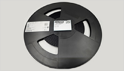
- Step1:Prepare product
-
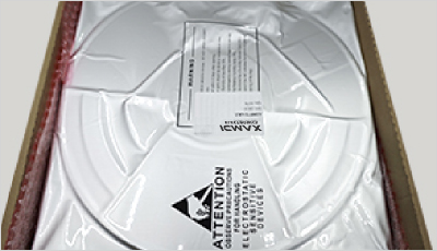
- Step2:Vacuum packaging
-
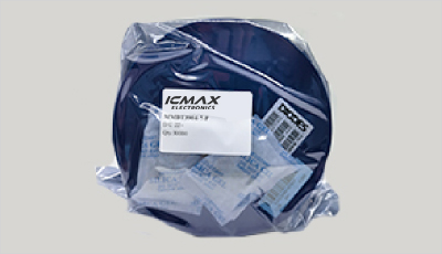
- Step3:Anti-static bag
-
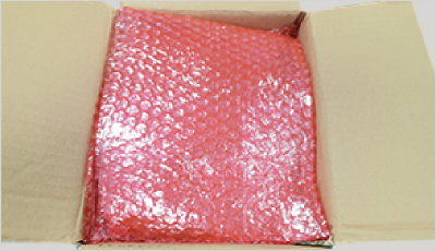
- Step4:Individual package
-
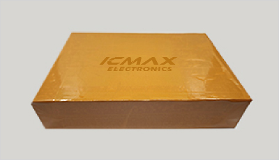
- Step5:Packaging box
-
- Step6:Barcode shipping label
Shipping starts at $40, but some countries will exceed $40. For example (South Africa, Brazil, India, Pakistan, Israel, etc.)
The basic freight (for package ≤0.5kg or corresponding volume) depends on the time zone and country.
Currently, our products are shipped through DHL, FedEx, SF, and UPS.
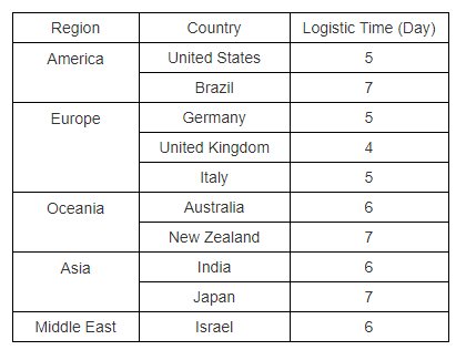
Delivery TimeOnce the goods are shipped, estimated delivery time depends on the shipping methods you chose:
FedEx International, 5-7 business days.
The following are some common countries' logistic time.
- Hot Sale
- Related Categories
- Include Parts
- Popular Search
- Voltage Regulators - Linear, Low Drop Out (LDO) Regulators(66836)
- Voltage Regulators - Linear Regulator Controllers(325)
- Voltage Regulators - Linear + Switching(1473)
- Voltage Regulators - DC DC Switching Regulators(35756)
- Voltage Reference(8428)
- V/F and F/V Converters(139)
- Thermal Management(515)
- Supervisors(41287)
- Special Purpose Regulators(4820)
- RMS to DC Converters(144)
The following parts include "TNY279GN" in Silicon Labs TNY279GN.
- Part Number
- Manufacturer
- Package
- Description
- LNK6407D-TL Power Integrations 8-SMD (7 Leads), Gull Wing IC OFFLINE SWITCH FLYBACK 8SMD
- LNK3204D-TL Power Integrations 8-SMD (7 Leads), Gull Wing IC OFFLINE SWITCH FLYBACK 8SMD
- SR10LG-G Microchip Technology 8-SMD (7 Leads), Gull Wing IC OFFLINE SWITCH FLYBACK 8SMD
- TNY285DG-TL Power Integrations 8-SMD (7 Leads), Gull Wing IC OFFLINE SWITCH FLYBACK 8SMD
- LNK304DN-TL Datasheet, Price, Stock & Alternatives | ICMASS Power Integrations 8-SMD (7 Leads), Gull Wing IC OFFLINE SWITCH FLYBACK 8SMD
- TNY285KG-TL Power Integrations 8-SMD (7 Leads), Gull Wing IC OFFLINE SWITCH FLYBACK 8SMD
- LNK3206D-TL Power Integrations 8-SMD (7 Leads), Gull Wing IC OFFLINE SWITCH FLYBACK 8SMD
- LNK623DG-TL Power Integrations 8-SMD (7 Leads), Gull Wing IC OFFLINE SWITCH FLYBACK 8SMD
- TNY286PG Power Integrations 8-SMD (7 Leads), Gull Wing IC OFFLINE SWITCH FLYBACK 8SMD
- LNK624DG-TL Power Integrations 8-SMD (7 Leads), Gull Wing IC OFFLINE SWITCH FLYBACK 8SMD
The following parts are popular search parts in Test and Measurement.
Inventory:0
Please send an inquiry. Send us your inquiry, and we will respond immediately.

- 1500+ Daily average RFQ Volume

- 20,000.000 Standard Product Unit

- 1800+ Worldwide Manufacturers

- 15,000+ In-stock Warehouse


