


NCEPower NCE9926

- Part No.:
- NCE9926
- Manufacturer:
- NCEPower
- Category:
- N-Channel MOSFETs
- Package:
- Description:
- NCE9926 — 20V/6A Dual N-Channel Power MOSFET (SOP-8)The NCE9926 is a dual N-Channel enhancement-mode power MOSFET from Wuxi NCE Power: two independent 20V/6A channels in one SOP-8. The headline spec is the 2.5V gate drive — RDS(on) is specified…
- Quantity:
-
Unit Price:$0
Ext Price:$0
- Payment:
-

- Shipping:
-


NCE9926 Information
- Specifications
- Product Details
- Comparison
- Tags
- Product attributes
- Attribute value
- Manufacturer:
- NCEPower
- Series:
- Package/Case:
- Packaging:
- SOP-8
- Product Status:
- Production
- FET Type:
- Industrial grade
- Technology:
- Trench双芯
- Drain to Source Voltage (Vdss):
- N+N
- Current - Continuous Drain (Id) @ 25°C:
- 20
- Drive Voltage (Max Rds On, Min Rds On):
- 6
- Rds On (Max) @ Id, Vgs:
- 0.75
- Vgs(th) (Max) @ Id:
- Gate Charge (Qg) (Max) @ Vgs:
- Vgs (Max):
- 20
- Input Capacitance (Ciss) (Max) @ Vds:
- 28
- FET Feature:
- 26
- Power Dissipation (Max):
- 37
- Operating Temperature:
- ±12
- Grade:
- 640
- Qualification:
- 10
- Mounting Type:
- 1.25
- Supplier Device Package:
NCE9926 — 20V/6A Dual N-Channel Power MOSFET (SOP-8)
The NCE9926 is a dual N-Channel enhancement-mode power MOSFET from Wuxi NCE Power: two independent 20V/6A channels in one SOP-8. The headline spec is the 2.5V gate drive — RDS(on) is specified at 2.5V, so a 3.3V or even 1.8V logic rail turns it on fully, not partially.
From what we see in Shenzhen (2025–2026), the 9926 family is the dual N-Channel workhorse behind battery protection boards and low-voltage load switches.
The most common design failure we're asked about isn't the part — it's the high-side N-Channel gate drive. When the source floats up to the rail, a battery-referenced MCU pin can't produce enough VGS, and the switch never fully turns on.
Both channels are independent (D1 and D2 on separate pins), which matters: for battery protection you connect D1 and D2 together on the PCB — back-to-back channels block current in both directions.
What Are the Technical Specifications of NCE9926?
| Parameter | Value |
|---|---|
| Type | Dual N-Channel Enhancement Mode Power MOSFET (Trench) |
| Package | SOP-8 (SO-8), 2500/reel, RoHS / halogen-free |
| Drain-Source Voltage (VDS) | 20V |
| Gate-Source Voltage (VGS) | ±10V |
| Continuous Drain Current (ID) | 6A per channel @ 25°C; 3.8A @ 100°C |
| Pulsed Drain Current (IDM) | 25A per channel |
| On-Resistance RDS(on) @ 4.5V | 28mΩ max |
| On-Resistance RDS(on) @ 2.5V | 37mΩ max |
| Gate Threshold Voltage (VGS(th)) | 0.6V to 1.5V (typ 1.2V) |
| Max Power Dissipation (PD) | 1.25W @ 25°C |
| Total Gate Charge (Qg) | 4nC typ @ 4.5V |
| Input Capacitance (Ciss) | 640pF typ |
| Operating Junction Temperature | -55°C to +150°C |
Key numbers that matter: the 2.5V RDS(on) spec is rare at this current level. VGS(th) sits at 0.6–1.5V, so the channel is fully enhanced well before 3.3V — unlike parts specified only at 4.5V or 10V, there's no "partially on" zone at logic levels.
Per the NCE9926 datasheet, 6A per channel at 28mΩ means about 1W of conduction loss at full load — and PD is only 1.25W. The SOP-8 package is the real limit.
Treat it as a 2–4A per channel workhorse with pulses up to 25A, not a continuous 6A part.
The 4nC gate charge per channel is tiny. Two MCU pins through 100Ω–1kΩ series resistors switch both channels cleanly at load-switch speeds.
When Should You Use (and NOT Use) the NCE9926?
✅ Use NCE9926 when:
- Battery protection with a DW01-class IC. Two channels tied drain-to-drain block charge and discharge paths independently — the standard 1S Li-ion protection topology. The 0.6–1.5V threshold matches what a protection IC can actually drive.
- Load switching from 1.8V–3.3V logic. With RDS(on) specified at 2.5V, an MCU GPIO turns the channel fully on. No level shifter, no driver stage.
- Low-voltage power gating (5V, 3.3V rails). The 20V rating covers the rail with room for transients, and the 25A pulse rating absorbs capacitive inrush.
- Two independent switches in one footprint. LED banks, motor half-bridges at low voltage, or dual-load gating — one SOP-8 replaces two SOT-23s and their PCB area.
- UPS and hard-switched circuits at moderate frequency. 4nC gate charge keeps driver losses low at tens of kHz.
❌ Don't use NCE9926 when:
- You need more than ~4A continuous per channel. The 1.25W PD budget runs out fast. Two channels in parallel help only if you control current sharing — otherwise step up to a TO-252 or a dual with a proper heatsink tab.
- Gate drive can exceed ±10V. A 12V rail with the gate pulled to ground puts 12V across VGS. Use a Zener clamp or divider.
- High-side switching above 3.3V logic. The part turns on, but an N-Channel's source floats with the load — you need a charge pump or level shifter. For simple high-side from 5V+, a P-Channel like NCE9435 is the easier answer.
- Sub-milliohm or high-current power stages (>10A). 28mΩ is a logic-level part's resistance, not a power stage's. Look at TO-252 or DPAK duals.
What Are the Alternatives to NCE9926?
| Model | Type | Key Difference | Best For |
|---|---|---|---|
| SI9926DY | Dual N-Ch, SOP-8 | 20V/6.5A, 30mΩ @ 4.5V, onsemi/TEMIC | Branded drop-in; same pin layout as NCE9926 |
| NCE9926A | Dual N-Ch, SOP-8 | 2.5V-specified PowerTrench-class update | Direct upgrade from the same manufacturer |
| AFN8205 | Dual N-Ch, SOT-23-6 | 20V/4A common-drain, the DW01 companion | Tiny battery-protection boards where SOP-8 is too big |
| NCE9926-VB | Dual N-Ch, SOP-8 | 26mΩ @ 4.5V, VBsemi-compatible | Second-source cross-reference, tighter RDS(on) |
| NCE9435 | Single P-Ch, SOP-8 | -30V/-5.1A, 4.5V drive | High-side switching without a gate driver |
The dual-N decision in one line: if the board is battery protection or sub-5V load switching, NCE9926 is the shape of the answer — two independent channels you tie into whatever topology you need. For simple high-side switching, the NCE9435 P-Channel avoids the floating-source drive problem entirely.
SOP-8 pinout: two independent channels — S1/G1 on pins 1–2, S2/G2 on pins 3–4, drains on pins 5–8 (D2 = 5–6, D1 = 7–8). For battery protection, tie D1 and D2 together on the PCB.
1S Li-ion protection topology: two channels in series between B- and P-, drains tied together. G1 (OC) opens on over-charge, G2 (OD) on over-discharge — each body diode blocks the direction it would otherwise leak, so both directions are cut when both gates are off.
RDS(on) per channel — the logic-drive advantage:
Dropping from 4.5V to 2.5V drive costs only ~30% on-resistance — the price of being fully specified at logic levels. Parts rated only at 4.5V pay the same penalty but unspecified.
What Are the Typical Applications of NCE9926?
1S Li-ion battery protection (DW01-class): The two channels connect drain-to-drain between the cell and the P+ terminal. One channel opens on over-discharge, the other on over-charge.
Because each body diode points the opposite way, current is blocked in both directions when both channels are off. This is the topology behind most 18650 protection boards.
Low-voltage load switching: At 3.3V or 5V rails, a GPIO drives the gate through a series resistor. With RDS(on) guaranteed at 2.5V, the channel is fully on — no partial enhancement, no headroom surprises.
Battery-powered instrument power gating: Two independent switches in one package let one part gate the main rail and the standby rail separately. The 4nC gate charge keeps both switches fast, and the 25A pulse rating swallows the inrush of a charging bulk capacitor.
UPS and hard-switched auxiliary circuits: The datasheet's listed applications include UPS and high-frequency hard switching — at tens of kHz the low gate charge keeps driver loss negligible.
Why Buy NCE9926 from ICMASS?
Tested at the threshold that matters. We batch-test VGS(th) and RDS(on) at 2.5V before shipping. In our experience (2025–2026), remarked duals are common — a part marked 9926 with a higher-threshold die inside fails exactly at the 2.5V measurement a logic-driven design depends on.
Cross-reference support for the whole dual-N family. Not sure whether your protection board wants NCE9926, SI9926DY, or a SOT-23-6 like AFN8205? Tell us the battery count, load current, and gate drive — we'll match the part.
BOM consolidation for battery products. The same 1S pack BOM carries the protection IC, the TP4056 charger, and the NCE9926 dual MOSFET. One shipment, one supplier, no cross-channel surprises.
Same-day dispatch, 5–10 days worldwide. Orders before 15:00 CST ship same day via DHL or FedEx.
Frequently Asked Questions About NCE9926
Q1: Can I replace an SI9926DY with an NCE9926 directly?
A: Yes — with one pinout check. The NCE9926 matches the onsemi/TEMIC SI9926DY layout (S1/G1 on pins 1–2, S2/G2 on 3–4, D2 on 5–6, D1 on 7–8). Some KEXIN-branded SI9926DY-HF parts use a different arrangement — verify against the specific datasheet before layout. Ratings are equivalent: 20V, ~6A, ~28mΩ.
Q2: Why does battery protection need two MOSFETs?
A: One MOSFET's body diode always conducts one way. A single channel that blocks discharge still lets the battery charge through its body diode, and vice versa. Two channels tied drain-to-drain (back-to-back) block current in both directions when both gates are off — that's the whole point of the dual configuration.
Q3: My high-side N-Channel switch never turns on — why?
A: The source floats up to the rail, so gate drive disappears. An N-Channel needs VGS above threshold, but when the source sits at the battery rail, a battery-referenced MCU pin can't pull the gate high enough. This is the #1 N-Channel high-side failure across the forums. Use a charge pump, a level shifter, or switch to a P-Channel like the NCE9435.
Q4: My protection board's second FET only conducts with "reversed" drain-source voltage — is it faulty?
A: No — MOSFETs are 4-quadrant devices. A channel turns on fully regardless of drain-source polarity as long as VGS is above threshold. In DW01-type circuits one FET seeing negative VDS while turning on is normal operation, not a defect. This confuses first-time battery-protection builders constantly.
Q5: Where should the gate pull-down resistors connect?
A: To each battery's own negative terminal, not a shared GND. If a converter ties one cell's negative to ground, gate voltages shift, both channels partially turn on, and cells at different voltages start equalizing through the MOSFETs — dangerous current that forum threads document with parts being destroyed. Reference gates to the cell they protect.
Q6: Can I drive NCE9926 from 1.8V logic?
A: Yes — this is the part's differentiator. VGS(th) is 0.6–1.5V and RDS(on) is specified at 2.5V, so 1.8V logic partially enhances and 3.3V turns it fully on. Compare with parts specified only at 4.5V — at 3.3V those run at unspecified, elevated resistance.
Q7: What's the real continuous current limit?
A: Budget 2–4A per channel; the package is the limit. The datasheet lists 6A @ 25°C, but PD is 1.25W and 6A at 28mΩ is about 1W — leaving almost no thermal margin. Treat 4A as the practical ceiling with good copper, and use the 25A pulse rating for transients only.
Q8: NCE9926 vs NCE9926A — what changed?
A: The -A is the current-generation die, optimized for 2.5V-specified drive. Same 20V/6A rating and SOP-8 pinout, with tighter RDS(on) characterization. The original NCE9926 remains widely stocked; the -A is what new production mostly ships as.
Q9: My simulation shows FET2 won't turn off — is the real circuit broken?
A: Probably a SPICE model artifact. In simulations, a floating source node can leak current through the substrate diode into the other FET's path — a sneak path that doesn't exist in the real circuit where the ground node stays at battery ground. Known issue when simulating DW01-class protection with generic models.
Q10: What happens if VGS exceeds 10V?
A: You're out of the ±10V absolute maximum — the gate oxide takes damage. In 12V+ rails, pull the gate to ground through a divider or clamp with a Zener. The low threshold means you never need more than ~5V of drive anyway.
| Image |
|
| Part Number | NCE9926 |
| Manufacturer | NCEPower |
| Series | |
| Package/Case | |
| Packaging | SOP-8 |
| Product Status | Production |
| FET Type | Industrial grade |
| Technology | Trench双芯 |
| Drain to Source Voltage (Vdss) | N+N |
| Current - Continuous Drain (Id) @ 25°C | 20 |
| Drive Voltage (Max Rds On, Min Rds On) | 6 |
| Rds On (Max) @ Id, Vgs | 0.75 |
| Vgs(th) (Max) @ Id | |
| Gate Charge (Qg) (Max) @ Vgs | |
| Vgs (Max) | 20 |
| Input Capacitance (Ciss) (Max) @ Vds | 28 |
| FET Feature | 26 |
| Power Dissipation (Max) | 37 |
| Operating Temperature | ±12 |
| Grade | 640 |
| Qualification | 10 |
| Mounting Type | 1.25 |
| Supplier Device Package |
User Guide
- Purchase & Inquiry
- Package
- Shipping Information
- Customer Review
You may place an order without registering to IC-MAX.COM
We strongly suggest you sign in before purchasing as you can track your order in real time.
For your convenience, we accept multiple payment methods in USD, including PayPal, Credit Card, and wire transfer.
RFQ (Request for Quotations)
It is recommended to request for quotations to get the latest prices and inventories about the part.
Our sales will reply to your request by email within 24 hours.
1. You'll receive an order information email in your inbox. (Please remember to check the spam folder if you didn't hear from us).
2. Since inventories and prices may fluctuate to some extent, the sales manager is going to reconfirm the order and let you know if there are any updates.
-
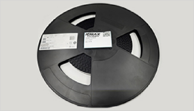
- Step1:Prepare product
-
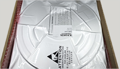
- Step2:Vacuum packaging
-
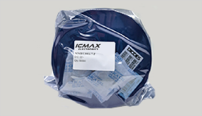
- Step3:Anti-static bag
-
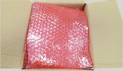
- Step4:Individual package
-
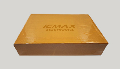
- Step5:Packaging box
-
- Step6:Barcode shipping label
Shipping starts at $40, but some countries will exceed $40. For example (South Africa, Brazil, India, Pakistan, Israel, etc.)
The basic freight (for package ≤0.5kg or corresponding volume) depends on the time zone and country.
Currently, our products are shipped through DHL, FedEx, SF, and UPS.
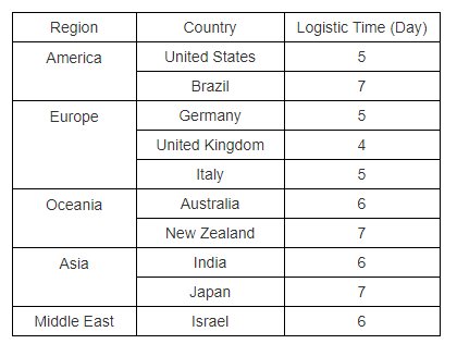
Delivery TimeOnce the goods are shipped, estimated delivery time depends on the shipping methods you chose:
FedEx International, 5-7 business days.
The following are some common countries' logistic time.
- Hot Sale
- Related Categories
- Include Parts
- Popular Search
The following parts include "NCE9926" in Silicon Labs NCE9926.
- Part Number
- Manufacturer
- Package
- Description
- BSZ180P03NS3EGATMA1 Infineon Technologies NCE9926 — 20V/6A Dual N-Channel Power MOSFET (SOP-8)The NCE9926 is a dual N-Channel enhancement-mode power MOSFET from Wuxi NCE Power: two independent 20V/6A channels in one SOP-8. The headline spec is the 2.5V gate drive — RDS(on) is specified…
- SIRA14DP-T1-GE3 Vishay Siliconix NCE9926 — 20V/6A Dual N-Channel Power MOSFET (SOP-8)The NCE9926 is a dual N-Channel enhancement-mode power MOSFET from Wuxi NCE Power: two independent 20V/6A channels in one SOP-8. The headline spec is the 2.5V gate drive — RDS(on) is specified…
- AO4419 Alpha & Omega Semiconductor Inc. NCE9926 — 20V/6A Dual N-Channel Power MOSFET (SOP-8)The NCE9926 is a dual N-Channel enhancement-mode power MOSFET from Wuxi NCE Power: two independent 20V/6A channels in one SOP-8. The headline spec is the 2.5V gate drive — RDS(on) is specified…
- SISA14BDN-T1-GE3 Vishay Siliconix NCE9926 — 20V/6A Dual N-Channel Power MOSFET (SOP-8)The NCE9926 is a dual N-Channel enhancement-mode power MOSFET from Wuxi NCE Power: two independent 20V/6A channels in one SOP-8. The headline spec is the 2.5V gate drive — RDS(on) is specified…
- PSMN9R5-30YLC,115 Nexperia USA Inc. NCE9926 — 20V/6A Dual N-Channel Power MOSFET (SOP-8)The NCE9926 is a dual N-Channel enhancement-mode power MOSFET from Wuxi NCE Power: two independent 20V/6A channels in one SOP-8. The headline spec is the 2.5V gate drive — RDS(on) is specified…
- BUK9Y21-40E,115 Nexperia USA Inc. NCE9926 — 20V/6A Dual N-Channel Power MOSFET (SOP-8)The NCE9926 is a dual N-Channel enhancement-mode power MOSFET from Wuxi NCE Power: two independent 20V/6A channels in one SOP-8. The headline spec is the 2.5V gate drive — RDS(on) is specified…
- RTQ035N03HZGTR Rohm Semiconductor NCE9926 — 20V/6A Dual N-Channel Power MOSFET (SOP-8)The NCE9926 is a dual N-Channel enhancement-mode power MOSFET from Wuxi NCE Power: two independent 20V/6A channels in one SOP-8. The headline spec is the 2.5V gate drive — RDS(on) is specified…
- FDMS7680 onsemi NCE9926 — 20V/6A Dual N-Channel Power MOSFET (SOP-8)The NCE9926 is a dual N-Channel enhancement-mode power MOSFET from Wuxi NCE Power: two independent 20V/6A channels in one SOP-8. The headline spec is the 2.5V gate drive — RDS(on) is specified…
- RQ3E180BNTB Rohm Semiconductor NCE9926 — 20V/6A Dual N-Channel Power MOSFET (SOP-8)The NCE9926 is a dual N-Channel enhancement-mode power MOSFET from Wuxi NCE Power: two independent 20V/6A channels in one SOP-8. The headline spec is the 2.5V gate drive — RDS(on) is specified…
- STL6N2VH5 STMicroelectronics NCE9926 — 20V/6A Dual N-Channel Power MOSFET (SOP-8)The NCE9926 is a dual N-Channel enhancement-mode power MOSFET from Wuxi NCE Power: two independent 20V/6A channels in one SOP-8. The headline spec is the 2.5V gate drive — RDS(on) is specified…
The following parts are popular search parts in Test and Measurement.
Inventory:50,000
Please send an inquiry. Send us your inquiry, and we will respond immediately.

- 1500+ Daily average RFQ Volume

- 20,000.000 Standard Product Unit

- 1800+ Worldwide Manufacturers

- 15,000+ In-stock Warehouse


