


NCEPower NCE30H12K

- Part No.:
- NCE30H12K
- Manufacturer:
- NCEPower
- Category:
- N-Channel MOSFETs
- Package:
- Description:
- NCE30H12K — 30V/120A N-Channel Power MOSFET (TO-252-2L)The NCE30H12K is a 30V, 120A N-channel enhancement-mode power MOSFET from Wuxi NCE Power, in a TO-252-2L package, datasheet v1.1. On-resistance is 4.5mΩ max at 10V, measured at a 20A drain …
- Quantity:
-
Unit Price:$0
Ext Price:$0
- Payment:
-

- Shipping:
-


NCE30H12K Information
- Specifications
- Product Details
- Comparison
- Tags
- Product attributes
- Attribute value
- Manufacturer:
- NCEPower
- Series:
- Package/Case:
- Packaging:
- TO-252
- Product Status:
- Production
- FET Type:
- Industrial grade
- Technology:
- Trench
- Drain to Source Voltage (Vdss):
- N
- Current - Continuous Drain (Id) @ 25°C:
- 30
- Drive Voltage (Max Rds On, Min Rds On):
- 120
- Rds On (Max) @ Id, Vgs:
- 1.6
- Vgs(th) (Max) @ Id:
- 3
- Gate Charge (Qg) (Max) @ Vgs:
- 3.5
- Vgs (Max):
- 4.2
- Input Capacitance (Ciss) (Max) @ Vds:
- 5
- FET Feature:
- Power Dissipation (Max):
- Operating Temperature:
- ±20
- Grade:
- 4120
- Qualification:
- 79
- Mounting Type:
- 120
- Supplier Device Package:
NCE30H12K — 30V/120A N-Channel Power MOSFET (TO-252-2L)
The NCE30H12K is a 30V, 120A N-channel enhancement-mode power MOSFET from Wuxi NCE Power, in a TO-252-2L package, datasheet v1.1. On-resistance is 4.5mΩ max at 10V, measured at a 20A drain current.
From what we see across Shenzhen reorders (2025–2026), this current class turns up when a TO-220 gets swapped for a surface-mount tab — same headline current, no through-hole step in the line.
Here's the number most people skip: the front page says 120A and the ratings table says 84A, and both describe the same device. The 84A row is specified at case temperature, not ambient.
Reverse the sheet's own arithmetic and the assumption behind that row falls out. 84A across a 1.25°C/W junction-to-case path implies about 8.5mΩ of hot resistance — roughly 1.9 times the 25°C maximum of 4.5mΩ.
Two more things worth knowing up front. There is no 4.5V RDS(on) row anywhere in this sheet, and the tab is the drain — it sits at your rail, not at ground.
What Are the Technical Specifications of NCE30H12K?
| Parameter | Value |
|---|---|
| Type | N-Channel Enhancement Mode Power MOSFET (trench) |
| Package | TO-252-2L (DPAK), tab = Drain |
| Drain-Source Voltage (VDS) | 30V |
| Gate-Source Voltage (VGS) | ±20V |
| Continuous Drain Current (ID) | 120A @ TC = 25°C |
| Continuous Drain Current (ID) | 84A @ TC = 100°C |
| Pulsed Drain Current (IDM) | 400A |
| RDS(on) @ VGS = 10V | 4.5mΩ max (typ 3.5mΩ, ID = 20A) |
| RDS(on) @ VGS = 4.5V | Not published — no row in the sheet |
| Gate Threshold (VGS(th)) | 1.0V min / 1.6V typ / 3.0V max |
| Forward Transconductance (gfs) | 50S min (VDS = 10V, ID = 20A) |
| Input / Output Capacitance | Ciss 4120pF / Coss 498pF / Crss 456pF |
| Total Gate Charge (Qg) | 79nC (VGS = 10V, VDS = 15V, ID = 20A) |
| Gate-Drain Charge (Qgd) | 18nC |
| Switching (td(on)/tr/td(off)/tf) | 11 / 10 / 38 / 11 ns (RGEN = 3Ω) |
| Body Diode Forward Voltage (VSD) | 1.2V max (IS = 20A) |
| Reverse Recovery (trr / Qrr) | 58ns / 115nC (IF = 60A, di/dt = 100A/µs) |
| Single-Pulse Avalanche Energy (EAS) | 350mJ (L = 0.5mH, Rg = 25Ω, Tj = 25°C) |
| Max Power Dissipation (PD) | 120W @ TC = 25°C |
| Thermal Resistance (RθJC) | 1.25°C/W |
| Operating Junction Temperature | −55°C to 175°C |
| Reel / Tape | Not stated on the sheet (bare-tab TO-252) |
The 120W dissipation rating and the 1.25°C/W thermal resistance are the same statement twice: (175 − 25) / 1.25 = 120W. That arithmetic holds together, and it also tells you the ratings table is built entirely on case temperature.
So is the 84A row. Work it backwards and the sheet's assumed hot resistance appears: (175 − 100) / 1.25 = 60W, and 60W / 84A² = 8.5mΩ. That's the number the manufacturer expects the die to have at temperature — 1.9 times the 25°C maximum.
The third row is a first-order derivation, not a printed spec: hold a 40°C/W board at 25°C ambient and the self-heating equation lands near 19A with a 125°C junction. A 65°C/W board halves that margin again.
Both currents burn within 8% of each other — 64.8W against 60W. The difference is where the heat leaves: one point assumes a case pinned at room temperature, the other assumes a case at 100°C. The line between them is just (175 − TC) / 1.25.
When Should You Use (and NOT Use) the NCE30H12K?
✅ Use NCE30H12K when:
- Your gate driver actually runs at 10V. The single RDS(on) row is specified at 10V and 20A. Give it that and the 4.5mΩ maximum holds.
- You have real copper under the tab. A 12–15mm thermal pad with a filled via array into an inner plane is what turns this package into a power device.
- You're replacing a TO-220 in a 12V or 24V system. 30V rating with margin for ringing, and the tab solders down instead of needing a screw and insulator.
- Burst current matters more than average current. 400A pulsed rating at a 300µs pulse width, against 84A continuous at a 100°C case.
- You're already committed to the NCE 30H family. Same footprint and pinout as the 30H10K and 30H15K, so a ladder change is a reflow change, not a re-layout.
❌ Don't use NCE30H12K when:
- Your gate drive tops out at 5V or 3.3V. There is no 4.5V row to design against. Partially enhanced is an uncharacterized state, and the temperature rise becomes yours to own. Use the 30H15K or 40H12K instead — both publish a 4.5V line.
- You need 100A continuous on a normal board. The 84A row already assumes a 100°C case, which is itself a heatsink problem. Design for tens of amps unless you have measured your own copper.
- Your load is inductive and unclamped. 350mJ of single-pulse avalanche is a real budget, but it is a 25°C-junction number. Hot, it shrinks. The 30H15K carries 1700mJ for the same footprint.
- Your rail is above 30V. Obvious, but people read the 120A and forget the 30V. The 40H12K is the same current class one voltage step up.
- You're stacking it in parallel and expecting the avalanche to share. Breakdown voltages differ between dice; the lowest-BV device avalanches first and takes the current alone.
What Are the Alternatives to NCE30H12K?
| Model | Type | Key Difference | Best For |
|---|---|---|---|
| NCE40H12K | N-Ch 40V/120A, TO-252-2L | Same 120A and same 1.25°C/W, but 4.0mΩ max at 10V and a published 7.0mΩ at 4.5V — lower resistance at a higher voltage | New designs at 24V rails; any board that wants a 4.5V gate line |
| NCE30H15K | N-Ch 30V/150A, TO-252-2L | 4.0mΩ at 10V and 5.0mΩ at 4.5V, EAS 1700mJ, 105A at a 100°C case — and 38nC of gate charge at its own test condition | Inductive loads and avalanche-heavy switching where ruggedness earns its price |
| NCE30H10K | N-Ch 30V/100A, TO-252-2L | 5.5mΩ max at 10V, 70A at a 100°C case, no 4.5V row — the entry step of the same family | Cost-driven designs that only need the lower current class |
| NCE0115K | N-Ch 100V/15A, TO-252-2L | Same package, one third of the current, more than three times the voltage (80mΩ at 10V) | 48V and 72V rails where the voltage rating is the whole point |
Here's the thing that costs people money: they buy the 30V part because the number is bigger, then discover their gate driver is 5V. The 30H12K is a 10V-drive device in a family where two of its three siblings publish 4.5V rows. Check the driver before the amp rating.
What does your rail actually allow?
Then the ranking flips. The 40V 40H12K has lower on-resistance than this 30V part — 4.0mΩ against 4.5mΩ at the same test conditions, with the same thermal path. Voltage class is not what sets resistance inside this family; die generation is.
Read the drawing against the sheet and one thing matters more than the pin order: pin 2 and the tab are the same net, and that net is the drain.
The tab is your switching node. Bolt it to a grounded chassis and you have shorted the supply through the device.
What Are the Typical Applications of NCE30H12K?
Battery pack disconnect and charge paths. A 30V rating fits 6-cell and 7-cell lithium packs with review, and the 4.5mΩ maximum keeps conduction loss low where the current actually flows. Keep the gate at a real 10V rail and size the copper for the average, not the peak.
Motor drive in 24V systems. E-bike controllers and small BLDC drives use this package as the phase switch. The 400A pulse rating covers commutation spikes; the 58ns reverse recovery on the body diode sets how much of that energy comes back as heat.
UPS and inverter low-voltage stages. NCE lists uninterruptible power supplies on the front page, and the 30V/120A combination is aimed at the battery-side switch. Two parts in parallel are common here — add gate resistors per device and expect the avalanche current to be unequal.
Replacing through-hole TO-220 switches. Same current class, surface-mount tab, no screw or insulator. The trade is thermal: a TO-220 bolts to a heatsink, this part sells heat only through board copper.
Why Buy NCE30H12K from ICMASS?
We sample-test NCE30H12K lots at the sheet's own condition: 4.5mΩ maximum at VGS = 10V and ID = 20A. That is the only on-resistance row the datasheet publishes, so it is the only one worth measuring against.
The clone market is active on this part number. VBsemi sells a NCE30H12K-VB in the same TO-252 outline, and its published rows include a low-voltage RDS(on) line the NCE original never printed.
A part that looks better at 4.5V than at 10V is a different die wearing a similar code.
We stock the TO-252 NCE ladder together — 30H10K, 30H12K, 30H15K and 40H12K — each with its official PDF on hand, so a family swap inside the same footprint is a stock question rather than a sourcing project.
Orders ship same day from Shenzhen. Volume pricing keeps a genuine 120A TO-252 competitive against clone stock, and we will say plainly when a 40V sibling is the better buy for your rail.
Frequently Asked Questions About NCE30H12K
Q1: How much current can the NCE30H12K actually carry continuously?
A: Far less than 120A, and less than 84A on a normal board. The 84A row assumes a case held at 100°C, which on a real board means removing roughly 60W through copper alone. Hold a 40°C/W board at 25°C ambient and the self-heating equation lands near 19A at a 125°C junction. Treat 120A as a die capability, not a board capability.
Q2: Can I drive the gate from a 5V logic pin or a 4.5V rail?
A: No — this part has no 4.5V characterization at all. The only RDS(on) row is at VGS = 10V, ID = 20A. The threshold is 1.0–3.0V, so a 5V drive will turn it partly on, but partly on is an unspecified resistance and the temperature rise is unmeasured. Use the 30H15K or 40H12K if your driver is 4.5V.
Q3: Why does the 40V NCE40H12K have lower on-resistance than this 30V part?
A: Because voltage class isn't what sets RDS(on) inside this family — die generation is. The 40H12K publishes 4.0mΩ max at 10V against the 30H12K's 4.5mΩ, at the same 20A test current, with the same 1.25°C/W thermal path and the same 120A headline. It also publishes a 4.5V row that the 30H12K lacks. If your rail allows 40V, it is the better part.
Q4: Is 350mJ of avalanche energy a lot?
A: It's a real budget, but read the test condition. The sheet states L = 0.5mH, Rg = 25Ω, Tj = 25°C. Avalanche capability falls as the junction starts hot, and EAS is a single-pulse number. For repetitive or hot avalanche, the 30H15K's 1700mJ is the family's rugged option.
Q5: What does the tab connect to, and can I screw it to a chassis?
A: The tab is the drain, and it is live. Pin 2 and the tab are the same net, so the tab swings with your switching node. Grounding it shorts the supply through the device. Solder it to a dedicated copper pad with thermal vias — never to a grounded plane.
Q6: Can I compare this part's 79nC gate charge with the 30H15K's 38nC directly?
A: Closely, yes. Both rows are measured to the same 10V gate endpoint at VDS = 15V; only the test current differs, 20A here against 30A there. So the 30H15K really does specify about half the gate charge at the same drive voltage. What you cannot do is carry the number to a different rail — gate-drain charge scales with the drain voltage you actually switch, so re-check it at your own VDD.
Q7: How much copper do I need under the tab?
A: A 12–15mm square pad with a filled via array into an inner plane is the practical target. Published measurements for DPAK-class parts put a bare 20mm-square pour at roughly 50°C/W board-to-air, and an optimized pad with vias at roughly 25°C/W. Beyond about 1 in² of copper the returns flatten out, so area gets you further than thickness.
Q8: Is the NCE30H12K good for paralleling?
A: It works, with two caveats. Breakdown voltages vary between dice, and in avalanche the lowest-BV device takes the current first — so the 350mJ rating is not multiplied by the number of parts you stack. Gate resistors per device are also needed to stop oscillation between gates. Share the current thermally and the arrangement behaves; assume it shares automatically and it won't.
Q9: Is a genuine NCE30H12K being sold under other brands?
A: Yes — VBsemi lists a NCE30H12K-VB in TO-252, and its spec rows include a low-voltage RDS(on) line the NCE original doesn't publish. A clone that is better on paper at 5V is a different die, not a better one. Match the marking and check that the only on-resistance row is the 10V one.
Q10: What does the v1.1 datasheet revision change?
A: The sheet we work from is v1.1, and the numbers here come from it. Cross-reference databases and distributor tables often carry older or rounded figures — dissipation ratings that are double the sheet's, or typical resistances presented as guaranteed maxima. When a listing and the PDF disagree, the PDF with the revision number on it wins.
| Image |

|
| Part Number | NCE30H12K |
| Manufacturer | NCEPower |
| Series | |
| Package/Case | |
| Packaging | TO-252 |
| Product Status | Production |
| FET Type | Industrial grade |
| Technology | Trench |
| Drain to Source Voltage (Vdss) | N |
| Current - Continuous Drain (Id) @ 25°C | 30 |
| Drive Voltage (Max Rds On, Min Rds On) | 120 |
| Rds On (Max) @ Id, Vgs | 1.6 |
| Vgs(th) (Max) @ Id | 3 |
| Gate Charge (Qg) (Max) @ Vgs | 3.5 |
| Vgs (Max) | 4.2 |
| Input Capacitance (Ciss) (Max) @ Vds | 5 |
| FET Feature | |
| Power Dissipation (Max) | |
| Operating Temperature | ±20 |
| Grade | 4120 |
| Qualification | 79 |
| Mounting Type | 120 |
| Supplier Device Package |
User Guide
- Purchase & Inquiry
- Package
- Shipping Information
- Customer Review
You may place an order without registering to IC-MAX.COM
We strongly suggest you sign in before purchasing as you can track your order in real time.
For your convenience, we accept multiple payment methods in USD, including PayPal, Credit Card, and wire transfer.
RFQ (Request for Quotations)
It is recommended to request for quotations to get the latest prices and inventories about the part.
Our sales will reply to your request by email within 24 hours.
1. You'll receive an order information email in your inbox. (Please remember to check the spam folder if you didn't hear from us).
2. Since inventories and prices may fluctuate to some extent, the sales manager is going to reconfirm the order and let you know if there are any updates.
-
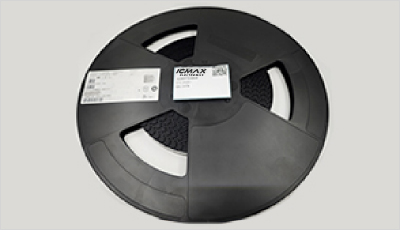
- Step1:Prepare product
-
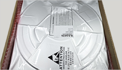
- Step2:Vacuum packaging
-
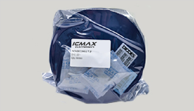
- Step3:Anti-static bag
-
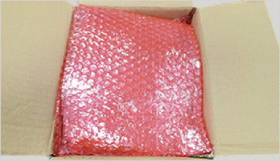
- Step4:Individual package
-
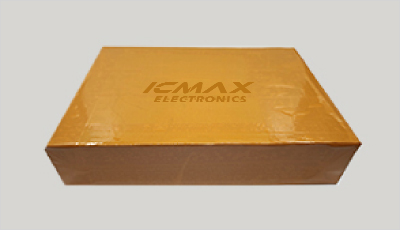
- Step5:Packaging box
-
- Step6:Barcode shipping label
Shipping starts at $40, but some countries will exceed $40. For example (South Africa, Brazil, India, Pakistan, Israel, etc.)
The basic freight (for package ≤0.5kg or corresponding volume) depends on the time zone and country.
Currently, our products are shipped through DHL, FedEx, SF, and UPS.
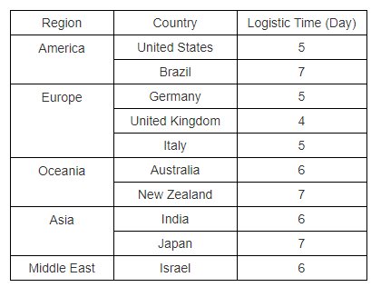
Delivery TimeOnce the goods are shipped, estimated delivery time depends on the shipping methods you chose:
FedEx International, 5-7 business days.
The following are some common countries' logistic time.
- Hot Sale
- Related Categories
- Include Parts
- Popular Search
The following parts include "NCE30H12K" in Silicon Labs NCE30H12K.
- Part Number
- Manufacturer
- Package
- Description
- BSZ180P03NS3EGATMA1 Infineon Technologies NCE30H12K — 30V/120A N-Channel Power MOSFET (TO-252-2L)The NCE30H12K is a 30V, 120A N-channel enhancement-mode power MOSFET from Wuxi NCE Power, in a TO-252-2L package, datasheet v1.1. On-resistance is 4.5mΩ max at 10V, measured at a 20A drain …
- SIRA14DP-T1-GE3 Vishay Siliconix NCE30H12K — 30V/120A N-Channel Power MOSFET (TO-252-2L)The NCE30H12K is a 30V, 120A N-channel enhancement-mode power MOSFET from Wuxi NCE Power, in a TO-252-2L package, datasheet v1.1. On-resistance is 4.5mΩ max at 10V, measured at a 20A drain …
- AO4419 Alpha & Omega Semiconductor Inc. NCE30H12K — 30V/120A N-Channel Power MOSFET (TO-252-2L)The NCE30H12K is a 30V, 120A N-channel enhancement-mode power MOSFET from Wuxi NCE Power, in a TO-252-2L package, datasheet v1.1. On-resistance is 4.5mΩ max at 10V, measured at a 20A drain …
- SISA14BDN-T1-GE3 Vishay Siliconix NCE30H12K — 30V/120A N-Channel Power MOSFET (TO-252-2L)The NCE30H12K is a 30V, 120A N-channel enhancement-mode power MOSFET from Wuxi NCE Power, in a TO-252-2L package, datasheet v1.1. On-resistance is 4.5mΩ max at 10V, measured at a 20A drain …
- PSMN9R5-30YLC,115 Nexperia USA Inc. NCE30H12K — 30V/120A N-Channel Power MOSFET (TO-252-2L)The NCE30H12K is a 30V, 120A N-channel enhancement-mode power MOSFET from Wuxi NCE Power, in a TO-252-2L package, datasheet v1.1. On-resistance is 4.5mΩ max at 10V, measured at a 20A drain …
- BUK9Y21-40E,115 Nexperia USA Inc. NCE30H12K — 30V/120A N-Channel Power MOSFET (TO-252-2L)The NCE30H12K is a 30V, 120A N-channel enhancement-mode power MOSFET from Wuxi NCE Power, in a TO-252-2L package, datasheet v1.1. On-resistance is 4.5mΩ max at 10V, measured at a 20A drain …
- RTQ035N03HZGTR Rohm Semiconductor NCE30H12K — 30V/120A N-Channel Power MOSFET (TO-252-2L)The NCE30H12K is a 30V, 120A N-channel enhancement-mode power MOSFET from Wuxi NCE Power, in a TO-252-2L package, datasheet v1.1. On-resistance is 4.5mΩ max at 10V, measured at a 20A drain …
- FDMS7680 onsemi NCE30H12K — 30V/120A N-Channel Power MOSFET (TO-252-2L)The NCE30H12K is a 30V, 120A N-channel enhancement-mode power MOSFET from Wuxi NCE Power, in a TO-252-2L package, datasheet v1.1. On-resistance is 4.5mΩ max at 10V, measured at a 20A drain …
- RQ3E180BNTB Rohm Semiconductor NCE30H12K — 30V/120A N-Channel Power MOSFET (TO-252-2L)The NCE30H12K is a 30V, 120A N-channel enhancement-mode power MOSFET from Wuxi NCE Power, in a TO-252-2L package, datasheet v1.1. On-resistance is 4.5mΩ max at 10V, measured at a 20A drain …
- STL6N2VH5 STMicroelectronics NCE30H12K — 30V/120A N-Channel Power MOSFET (TO-252-2L)The NCE30H12K is a 30V, 120A N-channel enhancement-mode power MOSFET from Wuxi NCE Power, in a TO-252-2L package, datasheet v1.1. On-resistance is 4.5mΩ max at 10V, measured at a 20A drain …
The following parts are popular search parts in Test and Measurement.
Inventory:50,000
Please send an inquiry. Send us your inquiry, and we will respond immediately.

- 1500+ Daily average RFQ Volume

- 20,000.000 Standard Product Unit

- 1800+ Worldwide Manufacturers

- 15,000+ In-stock Warehouse


