


NCEPower NCE30H10K

- Part No.:
- NCE30H10K
- Manufacturer:
- NCEPower
- Category:
- N-Channel MOSFETs
- Package:
- Description:
- NCE30H10K — 30V/100A N-Channel Power MOSFET (TO-252)The NCE30H10K is a 30V, 100A N-Channel power MOSFET from Wuxi NCE Power in TO-252 (DPAK).
- Quantity:
-
Unit Price:$0
Ext Price:$0
- Payment:
-

- Shipping:
-


NCE30H10K Information
- Specifications
- Product Details
- Comparison
- Tags
- Product attributes
- Attribute value
- Manufacturer:
- NCEPower
- Series:
- Package/Case:
- Packaging:
- TO-252
- Product Status:
- Production
- FET Type:
- Industrial grade
- Technology:
- Trench
- Drain to Source Voltage (Vdss):
- N
- Current - Continuous Drain (Id) @ 25°C:
- 30
- Drive Voltage (Max Rds On, Min Rds On):
- 100
- Rds On (Max) @ Id, Vgs:
- 1.6
- Vgs(th) (Max) @ Id:
- 4
- Gate Charge (Qg) (Max) @ Vgs:
- 5.5
- Vgs (Max):
- 5
- Input Capacitance (Ciss) (Max) @ Vds:
- 8
- FET Feature:
- Power Dissipation (Max):
- Operating Temperature:
- ±20
- Grade:
- 3400
- Qualification:
- 70
- Mounting Type:
- 110
- Supplier Device Package:
NCE30H10K - 30V/100A N-Channel Power MOSFET (TO-252)
The NCE30H10K is a 30V, 100A N-Channel power MOSFET from Wuxi NCE Power in TO-252 (DPAK). RDS(on) is 5.5mΩ max @ 10V - the part that carries current when the load switch and logic-level parts can't.
From our Shenzhen distribution work (2025–2026), the 30H10K sits in a specific socket: motor drives, BMS discharge paths, and inverter stages where the current is real and the gate comes from a proper driver.
The spec that matters most is the combination - 100A rating means I²R loss is 55W at full current. The datasheet number is only true on a well-thermalized board.
What Are the Technical Specifications of NCE30H10K?
| Parameter | Value |
|---|---|
| Type | N-Channel Enhancement Mode Power MOSFET (Trench) |
| Package | TO-252-2L (DPAK), surface mount |
| Drain-Source Voltage (VDS) | 30V |
| Gate-Source Voltage (VGS) | ±20V |
| Continuous Drain Current (ID) | 100A @ 25°C (package- and board-limited) |
| On-Resistance RDS(on) @ 10V | 5.5mΩ max (typ 4mΩ) |
| On-Resistance RDS(on) @ 4.5V | 8mΩ typ |
| Gate Threshold Voltage (VGS(th)) | 3V typ (per NCE datasheet) |
| Max Power Dissipation (PD) | 110W @ 25°C (case temperature) |
| Total Gate Charge (Qg) | 70nC @ 4.5V |
| Input Capacitance (Ciss) | 3.4nF |
| Output Capacitance (Coss) | 356pF |
| Operating Junction Temperature | -55°C to +175°C |
Key numbers that matter: do the loss math before you trust the 100A rating. At 50A, I²R = 13.75W; at 100A it's 55W. The 110W PD rating assumes the case stays cool - on a bare TO-252 pad you're nowhere near that.
The gate side is a driver's part, not an MCU's: VGS(th) typ 3V and 70nC gate charge mean a GPIO through a resistor will hold the die in the linear region and roast it. Budget a gate driver and low-impedance drive at 10V.
Per the NCE30H10K datasheet, the 4.5V drive figure exists, but this is a 10V-driven device in practice - the 5.5mΩ max rating is at VGS = 10V.
When Should You Use (and NOT Use) the NCE30H10K?
✅ Use NCE30H10K when:
- DC motor drive and H-bridges below 30V. Brush motors, e-bike hubs, and 12V/24V actuators pull 10–100A peaks - the 100A rating with 5.5mΩ is exactly this class.
- BMS discharge and protection paths. High-current pack protection where a logic-level dual like the NCE9926 runs out of headroom.
- Low-voltage inverter and UPS stages. The datasheet's listed applications - hard-switched circuits, UPS, power inverters - all assume a real gate driver.
- DC-DC synchronous rectification at 30V-class rails. Low RDS(on) and 70nC Qg balance conduction vs switching loss at tens of kHz.
- Hot-swap and load stages that need avalanche margin. The trench cell is avalanche-characterized, absorbing inductive kicks without dying.
❌ Don't use NCE30H10K when:
- You're driving the gate from an MCU pin. 70nC and 3V threshold mean the pin sits in the linear region during every edge. Use NCE9926 (2.5V-specified, 4nC) or add a proper driver.
- High-side switching without a level shifter. N-Channel high-side at 24V needs the gate 10V above the floating source. For simple high-side, use a P-Channel like NCE9435.
- The board can't dissipate 15W+. 30A through 5.5mΩ is already 5W. If the layout is copper-starved, the 100A rating is fiction.
- Rails above 30V. The rating is hard at 30V - flyback from motors will exceed it. Step to a 40V/60V-class trench part.
What Are the Alternatives to NCE30H10K?
| Model | Type | Key Difference | Best For |
|---|---|---|---|
| NCE30H10K-VB | N-Ch, TO-252 | 2mΩ @ 10V, Vth ~1.9V | Lower-loss cross-reference; verify against official datasheet |
| NCE9926 | Dual N-Ch, SOP-8 | 20V/6A, 2.5V logic drive | Low-current logic-driven switching and battery protection |
| NCE9435 | Single P-Ch, SOP-8 | -30V/-5.1A, 4.5V drive | High-side load switching without a gate driver |
| IRLR2905-family | N-Ch, TO-252 | 55V/42A, logic-level | Higher voltage, logic-level TO-252 sockets |
| NCE40H12K | N-Ch, TO-252 | 40V-class, higher voltage headroom | 24V systems with margin for motor flyback |
The power-stage decision in one line: 30H10K when the current is real (10A+) and a driver exists; NCE9926 when logic drives directly; NCE9435 when the switch is high-side and simple.
TO-252 (DPAK) pinout: pin 1 Gate, pin 2 Drain, pin 3 Source, tab = Drain - the standard N-Channel TO-252 arrangement. The tab is the thermal path: it's electrically Drain and must be soldered to a copper pour.
Low-side motor drive: the 30H10K switches the motor's return path to GND; a gate driver delivers 10V with 2–4A peak to charge the 70nC gate. The freewheel diode across the motor clamps flyback when the FET opens. Dead time is mandatory when two such stages form an H-bridge.
RDS(on) across the NCE power line - conduction loss at 10A:
At 10A, the 30H10K dissipates 0.55W - a tenth of the 9435's 5.3W in the same job. The TO-252's tab and copper pour are what make the difference.
What Are the Typical Applications of NCE30H10K?
DC motor H-bridge (12V/24V): Four NCE30H10Ks form a classic N-Channel H-bridge with a driver IC. At 30A per FET the conduction loss is 5W each - the TO-252 tab pours and driver dead-time control are what keep the bridge alive through locked-rotor peaks.
BMS high-current discharge path: In a 1–7S pack discharge stage, the 30H10K replaces multiple paralleled small FETs. One 100A-rated die with proper copper replaces three or four 30A parts and their gate drivers.
Low-voltage inverter stage: The datasheet lists UPS and inverters. At tens of kHz, the 70nC gate charge needs a driver with a few amps of peak current, and the low RDS(on) keeps the switching-stage conduction loss small.
Battery tool and e-bike power stages: High-current interrupted flows - throttle, brake, and boost paths. The avalanche rating absorbs the motor's flyback without an external clamp diode in many designs.
Why Buy NCE30H10K from ICMASS?
Lot-tested for the ratings that burn. We verify RDS(on) at 10V and VGS(th) on every lot before shipping. At 100A class, a remarked die with 2× the resistance fails exactly where it hurts - heat.
Cross-reference support for the whole NCE power line. Not sure whether your stage wants the 30H10K, the 40H-class, or a paralleled SOP-8 pair? Send us the rail voltage, peak current, and switching frequency - we'll match the die.
BOM consolidation for power products. The same motor-drive BOM carries the 30H10K power stage, the NCE9926 logic switch, and the NCE9435 high-side rail. One shipment covers the entire FET population.
Same-day dispatch, 5–10 days worldwide. Orders before 15:00 CST ship same day via DHL or FedEx.
Frequently Asked Questions About NCE30H10K
Q1: Is 100A really a continuous rating?
A: Only under datasheet conditions - cool case, low ambient. The 100A figure assumes the case is held at 25°C. In the real world, I²R at 100A is 55W, so the package and PCB thermal path decide what you actually get. Budget 30–60A continuous on a well-thermalized board, with 100A as a peak capability.
Q2: Can I drive NCE30H10K directly from an MCU pin?
A: No - and this is the most common way to kill it. With VGS(th) typ 3V and 70nC gate charge, a GPIO holds the die in the linear region during switching, dumping power into the FET instead of the load. Use a gate driver (peak current of 2–4A is typical for this Qg) at 10V drive.
Q3: What gate resistor value should I use?
A: 10Ω is the typical starting point; 5Ω for fast switching. Too large a resistor forms an RC with the 3.4nF input capacitance and keeps the FET in the ohmic region too long - excess heat. Too small invites ringing and gate-oxide stress. For paralleled FETs, each die gets its own gate resistor.
Q4: Can I parallel NCE30H10Ks for more current?
A: Yes, but each FET needs its own gate resistor. Thresholds differ between dies; without individual resistors, the lower-threshold FET grabs the current and dies first. With separate gate resistors, parallel devices share reasonably well. The TO-252 tab pours still need to be symmetric for thermal sharing.
Q5: How thick does the PCB trace need to be for 100A?
A: Standard copper foil won't carry it - plan a copper bar or heavy pours. Roughly 15mm² of copper cross-section is the rule of thumb for 100A. On a typical 2oz (70µm) layer, that's a 215mm-wide trace - in practice, solder copper bars or bus bars over the FET tabs.
Q6: NCE30H10K vs NCE9926 vs NCE9435 - which do I need?
A: 30H10K for the power path, 9926 for logic-driven switching, 9435 for high-side. The 30H10K carries 10–100A with a real driver; the NCE9926's 2.5V-specified channels handle 2–4A from GPIOs; the NCE9435 does high-side P-Channel without a level shifter. Most boards need two of the three.
Q7: My motor drive keeps blowing the FETs - what should I check?
A: Check three things: dead time, gate drive, and layout inductance. At 100A, shoot-through (both FETs on) vaporizes dies in microseconds - dead time is mandatory. Undervoltage on the driver leaves FETs half-on, another classic killer. And source-lead inductance induces voltages that can spike the gate oxide - keep the driver low-impedance and the layout tight.
Q8: How do I calculate the heatsink requirement?
A: I²R first, then the thermal budget. At 40A, loss is 8.8W (40² × 5.5mΩ). The TO-252 junction-to-case is low, but junction-to-ambient on bare copper is terrible - size the pour or heatsink so junction stays under ~125°C (with 175°C max, keep 50°C margin).
Q9: My switch burns on power-up, not during operation - why?
A: Inrush into the output capacitance or motor is exceeding the safe area. A discharged capacitor bank looks like a short - 100A-capable die will charge it violently. Add soft-start (slower gate edge or an inrush limiter) and check the SOA during the transient, not just steady state.
Q10: What's the difference between NCE30H10K and NCE30H10K-VB?
A: The -VB is a VBsemi-sourced cross-reference with a lower-loss die: about 2mΩ @ 10V and Vth ~1.9V. Functionally compatible in the TO-252 socket, but the lower threshold changes drive requirements - verify against the specific datasheet before you swap it into a design tuned for the NCE original.
| Image |

|
| Part Number | NCE30H10K |
| Manufacturer | NCEPower |
| Series | |
| Package/Case | |
| Packaging | TO-252 |
| Product Status | Production |
| FET Type | Industrial grade |
| Technology | Trench |
| Drain to Source Voltage (Vdss) | N |
| Current - Continuous Drain (Id) @ 25°C | 30 |
| Drive Voltage (Max Rds On, Min Rds On) | 100 |
| Rds On (Max) @ Id, Vgs | 1.6 |
| Vgs(th) (Max) @ Id | 4 |
| Gate Charge (Qg) (Max) @ Vgs | 5.5 |
| Vgs (Max) | 5 |
| Input Capacitance (Ciss) (Max) @ Vds | 8 |
| FET Feature | |
| Power Dissipation (Max) | |
| Operating Temperature | ±20 |
| Grade | 3400 |
| Qualification | 70 |
| Mounting Type | 110 |
| Supplier Device Package |
User Guide
- Purchase & Inquiry
- Package
- Shipping Information
- Customer Review
You may place an order without registering to IC-MAX.COM
We strongly suggest you sign in before purchasing as you can track your order in real time.
For your convenience, we accept multiple payment methods in USD, including PayPal, Credit Card, and wire transfer.
RFQ (Request for Quotations)
It is recommended to request for quotations to get the latest prices and inventories about the part.
Our sales will reply to your request by email within 24 hours.
1. You'll receive an order information email in your inbox. (Please remember to check the spam folder if you didn't hear from us).
2. Since inventories and prices may fluctuate to some extent, the sales manager is going to reconfirm the order and let you know if there are any updates.
-
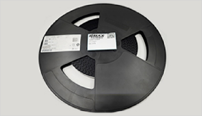
- Step1:Prepare product
-
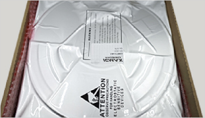
- Step2:Vacuum packaging
-
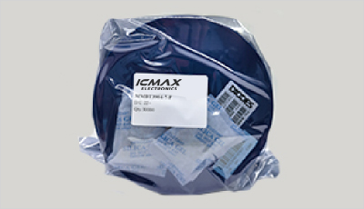
- Step3:Anti-static bag
-
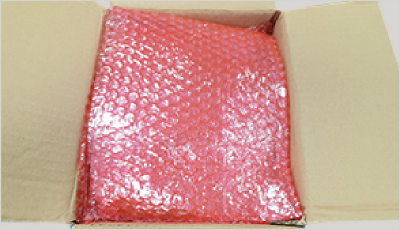
- Step4:Individual package
-
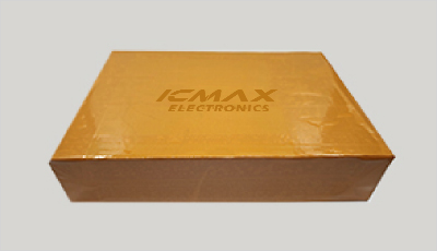
- Step5:Packaging box
-
- Step6:Barcode shipping label
Shipping starts at $40, but some countries will exceed $40. For example (South Africa, Brazil, India, Pakistan, Israel, etc.)
The basic freight (for package ≤0.5kg or corresponding volume) depends on the time zone and country.
Currently, our products are shipped through DHL, FedEx, SF, and UPS.
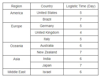
Delivery TimeOnce the goods are shipped, estimated delivery time depends on the shipping methods you chose:
FedEx International, 5-7 business days.
The following are some common countries' logistic time.
- Hot Sale
- Related Categories
- Include Parts
- Popular Search
The following parts include "NCE30H10K" in Silicon Labs NCE30H10K.
- Part Number
- Manufacturer
- Package
- Description
- BSZ180P03NS3EGATMA1 Infineon Technologies NCE30H10K — 30V/100A N-Channel Power MOSFET (TO-252)The NCE30H10K is a 30V, 100A N-Channel power MOSFET from Wuxi NCE Power in TO-252 (DPAK).
- SIRA14DP-T1-GE3 Vishay Siliconix NCE30H10K — 30V/100A N-Channel Power MOSFET (TO-252)The NCE30H10K is a 30V, 100A N-Channel power MOSFET from Wuxi NCE Power in TO-252 (DPAK).
- AO4419 Alpha & Omega Semiconductor Inc. NCE30H10K — 30V/100A N-Channel Power MOSFET (TO-252)The NCE30H10K is a 30V, 100A N-Channel power MOSFET from Wuxi NCE Power in TO-252 (DPAK).
- SISA14BDN-T1-GE3 Vishay Siliconix NCE30H10K — 30V/100A N-Channel Power MOSFET (TO-252)The NCE30H10K is a 30V, 100A N-Channel power MOSFET from Wuxi NCE Power in TO-252 (DPAK).
- PSMN9R5-30YLC,115 Nexperia USA Inc. NCE30H10K — 30V/100A N-Channel Power MOSFET (TO-252)The NCE30H10K is a 30V, 100A N-Channel power MOSFET from Wuxi NCE Power in TO-252 (DPAK).
- BUK9Y21-40E,115 Nexperia USA Inc. NCE30H10K — 30V/100A N-Channel Power MOSFET (TO-252)The NCE30H10K is a 30V, 100A N-Channel power MOSFET from Wuxi NCE Power in TO-252 (DPAK).
- RTQ035N03HZGTR Rohm Semiconductor NCE30H10K — 30V/100A N-Channel Power MOSFET (TO-252)The NCE30H10K is a 30V, 100A N-Channel power MOSFET from Wuxi NCE Power in TO-252 (DPAK).
- FDMS7680 onsemi NCE30H10K — 30V/100A N-Channel Power MOSFET (TO-252)The NCE30H10K is a 30V, 100A N-Channel power MOSFET from Wuxi NCE Power in TO-252 (DPAK).
- RQ3E180BNTB Rohm Semiconductor NCE30H10K — 30V/100A N-Channel Power MOSFET (TO-252)The NCE30H10K is a 30V, 100A N-Channel power MOSFET from Wuxi NCE Power in TO-252 (DPAK).
- STL6N2VH5 STMicroelectronics NCE30H10K — 30V/100A N-Channel Power MOSFET (TO-252)The NCE30H10K is a 30V, 100A N-Channel power MOSFET from Wuxi NCE Power in TO-252 (DPAK).
The following parts are popular search parts in Test and Measurement.
Inventory:50,000
Please send an inquiry. Send us your inquiry, and we will respond immediately.

- 1500+ Daily average RFQ Volume

- 20,000.000 Standard Product Unit

- 1800+ Worldwide Manufacturers

- 15,000+ In-stock Warehouse


