


NCEPower NCE3010S

- Part No.:
- NCE3010S
- Manufacturer:
- NCEPower
- Category:
- N-Channel MOSFETs
- Package:
- Description:
- NCE3010S — 30V/10A N-Channel Power MOSFET (SOP-8)The NCE3010S is a 30V/10A trench N-Channel MOSFET in SOP-8 — 12mΩ max at 10V, 16mΩ max at 4.5V, 32.5nC gate charge, from Wuxi NCE Power.From what we see across Shenzhen lots (2025&nda…
- Quantity:
-
Unit Price:$0
Ext Price:$0
- Payment:
-

- Shipping:
-


NCE3010S Information
- Specifications
- Product Details
- Comparison
- Tags
- Product attributes
- Attribute value
- Manufacturer:
- NCEPower
- Series:
- Package/Case:
- Packaging:
- SOP-8
- Product Status:
- Production
- FET Type:
- Industrial grade
- Technology:
- Trench
- Drain to Source Voltage (Vdss):
- N
- Current - Continuous Drain (Id) @ 25°C:
- 30
- Drive Voltage (Max Rds On, Min Rds On):
- 10
- Rds On (Max) @ Id, Vgs:
- 1.6
- Vgs(th) (Max) @ Id:
- 8
- Gate Charge (Qg) (Max) @ Vgs:
- 12
- Vgs (Max):
- 11
- Input Capacitance (Ciss) (Max) @ Vds:
- 16
- FET Feature:
- Power Dissipation (Max):
- Operating Temperature:
- ±20
- Grade:
- 1550
- Qualification:
- 13
- Mounting Type:
- 2.5
- Supplier Device Package:
NCE3010S — 30V/10A N-Channel Power MOSFET (SOP-8)
The NCE3010S is a 30V/10A trench N-Channel MOSFET in SOP-8 — 12mΩ max at 10V, 16mΩ max at 4.5V, 32.5nC gate charge, from Wuxi NCE Power.
From what we see across Shenzhen lots (2025–2026), 30V SOP-8 parts like this ship mostly into cordless tool boards, appliance load switches, small inverters, and LED drivers — the class that the AO4496/FDS6690-era sockets used to own.
The number that gets quoted wrong: 10A. Per the datasheet (V4.0), that's a TC = 25°C rating. It derates to 7A at 100°C, and the SOP-8 envelope is 2.5W — with the fine print that the 50°C/W thermal number is measured for t ≤ 10 seconds on FR4.
The spec that doesn't get quoted enough: the 4.5V row exists, but it's tested at 5A, not 10A. This is a 5V-logic part. Gate threshold runs up to 3V, so a 3.3V GPIO sits outside the guaranteed window — plan 5V drive.
What Are the Technical Specifications of NCE3010S?
| Parameter | Value |
|---|---|
| Type | N-Channel Enhancement Mode Power MOSFET (Trench) |
| Package | SOP-8 (SOIC-8, 150 mil) |
| Drain-Source Voltage (VDS) | 30V |
| Gate-Source Voltage (VGS) | ±20V |
| Continuous Drain Current (ID) | 10A @ TC = 25°C |
| Continuous Drain Current (ID) | 7A @ TC = 100°C |
| Pulsed Drain Current (IDM) | 50A |
| On-Resistance RDS(on) @ 10V | 8mΩ typ / 12mΩ max (ID = 10A) |
| On-Resistance RDS(on) @ 4.5V | 11mΩ typ / 16mΩ max (ID = 5A) |
| Gate Threshold Voltage (VGS(th)) | 1V to 3V (typ 1.6V) |
| Max Power Dissipation (PD) | 2.5W |
| Thermal Resistance RθJA | 50°C/W (FR4, surface mounted, t ≤ 10s) |
| Total Gate Charge (Qg) | 32.5nC @ 10V (Qgs 5nC / Qgd 6nC) |
| Input Capacitance (Ciss) | 1550pF (1100–2100pF, VDS = 15V) |
| Output Capacitance (Coss) | 300pF (VDS = 15V) |
| Switching Times | td(on) 30ns / tr 20ns / td(off) 100ns / tf 80ns |
| Body Diode Forward Voltage (VSD) | 1.2V max (IS = 10A) |
| Operating Junction Temperature | -55°C to +150°C |
| Avalanche | Fully characterized (no numeric EAS published) |
Key numbers that matter: per the NCE3010S datasheet (V4.0), RDS(on) is guaranteed at two gate voltages — 12mΩ max at 10V/10A and 16mΩ max at 4.5V/5A. The 4.5V test current is half the 10V test current, which tells you where the die's saturation curve sits.
Why does the 2.5W envelope matter? 2.5W at 50°C/W puts the junction at 150°C in a 25°C room — and that 50°C/W is the 10-second number. Real boards run 80–125°C/W steady-state, so the honest continuous budget is closer to 1W than 2.5W.
The avalanche note is honest: the datasheet says "fully characterized avalanche voltage and current" but publishes no numeric EAS. Treat it as a margin, not a spec — for inductive loads, keep the freewheeling clamp path.
When Should You Use (and NOT Use) the NCE3010S?
✅ Use NCE3010S when:
- 5V-logic load switches. RDS(on) is guaranteed at 4.5V, so a 5V MCU GPIO or 5V rail drives it fully enhanced. Relay, fan, solenoid, and heater switching on 12V/24V rails is the natural socket.
- Cordless tool and appliance power boards at 10-30W. 20V-max tool packs (5S, 21V charge) sit comfortably inside the 30V rating — the class leader in Shenzhen for low-side switching in compact SMD power stages (2025–2026), replacing SO-8 legacy parts at lower cost.
- UPS and power-switching circuits at moderate frequency. The datasheet's own application list — 32.5nC gate charge keeps a real driver happy into the hundreds of kHz.
- Parallel pairs for higher current. Two parts share the load with equal gate traces; the standard SO-8 pinout (pins 1-3 Source, 4 Gate, 5-8 Drain) makes the layout symmetric.
- Sockets currently running AO4496/FDS6690-class parts. Same package, same voltage/current class, and the 4.5V guarantee line matches what those parts promised.
❌ Don't use NCE3010S when:
- Driving from a 3.3V MCU GPIO. VGS(th) runs to 3V and RDS(on) is only specified at 4.5V and 10V — a 3.3V rail is outside the guaranteed window. Use a 2.5V-specified part or add a gate driver.
- Sustained 10A without PCB copper. 10A at 12mΩ is 1.2W of conduction loss — half the 2.5W envelope before you add switching loss. Without ≥100mm² of drain copper and thermal vias, the junction cooks.
- Raw 24V battery rails with transients. A 24V lead-acid float charge sits at 28.8V; 30V leaves under 1.2V of headroom for spikes. For 24V systems with real inductance, step to a 40V or 60V part (the NCE6008AS-class).
- High-frequency SMPS synchronous rectification. No body-diode trr is published, and 1550pF Ciss needs a serious driver. This is a switching part, not an SR part.
- Automotive load-dump exposure. A 40V load dump will punch through 30V — add a TVS or pick a 40V+ rated part for anything near the alternator.
What Are the Alternatives to NCE3010S?
| Model | Type | Key Difference | Best For |
|---|---|---|---|
| NCE3015S | N-Ch, SOP-8 | 30V/15A, same family, one step up | Headroom without a redesign |
| NCE3018AS | N-Ch, SOP-8 | 30V/18A, 7mΩ max @10V, 10mΩ @4.5V | The low-RDS(on) top of the family |
| AO4496 | N-Ch, SO-8 | 30V/10A class (AOS), the legacy socket | Drop-in cross-reference checks |
| FDS6690 | N-Ch, SO-8 | 30V/10A class, 10mΩ-class (onsemi legacy) | Legacy BOM second-source |
| BSC103N03LSG | N-Ch, SuperSO8 | ~10mΩ (Infineon), but leadless 5×6 package | Performance, with a re-layout |
| 40V/60V class | N-Ch, SOP-8 | NCE6008AS-family, same pinout | Raw 24V rails and hot-swap |
The 30V SOP-8 decision in one line: the 3010S sits at the 10A entry point of the NCE 30V family — the 3015S and 3018AS are the same package and pinout with bigger dies, and the drop-in check is the RDS(on) number at your actual gate voltage.
Here's the thing to check before substitution: the gate-drive row. A part that only specifies 10V (like the 60V NCE6008AS) is not a drop-in for a 4.5V-specified socket — the 3010S is, because its 4.5V row matches the legacy logic-level parts.
From what we see in Shenzhen (2025–2026), 30V SO-8 sockets that started on AO4496 or FDS6690 migrate to domestic parts like this for cost.
The migration fails most often when the new part is driven at the old part's gate voltage without checking the RDS(on) row. Same pinout, different guarantee.
SOP-8 pinout: pins 1–3 Source, pin 4 Gate, pins 5–8 Drain — the standard single-MOSFET arrangement shared across the whole SO-8 class, including the AO4496/FDS6690 legacy sockets and the NCE3015S/3018AS family steps.
12V low-side switch with 5V logic: the MCU GPIO drives the gate through RG; the 10k pull-down keeps the gate off during power-up when the MCU is still unconfigured.
Source pins 1–3 tie to ground, drain pins 5–8 to the load. The clamp diode across the load absorbs the inductive kick when a relay or solenoid opens.
NCE3010S RDS(on) max at the two guaranteed drive points (datasheet V4.0):
The 4.5V row is what makes this a 5V-logic part. A 3.3V rail is not a guarantee point — it sits below the 4.5V specification and inside the VGS(th) range.
Conduction loss at 12mΩ max — calculated from the datasheet, not measured:
Even at 10A, conduction loss alone eats half the 2.5W envelope — before switching loss and before the steady-state thermal reality (the 50°C/W number is a 10-second rating).
What Are the Typical Applications of NCE3010S?
5V-logic low-side switching in appliances: A 5V MCU rail switches a 12V relay or fan through the 3010S — the 4.5V guarantee is the whole point, and conduction loss at 1-2A is under 50mW.
20V-max cordless tool and appliance boards: The workhorse low-side switch in compact SMD power stages (2025–2026 Shenzhen market). 5S tool packs charge to 21V — well inside the 30V rating with the body diode handling the commutating path.
UPS power-switching sections: The datasheet lists UPS as a target application. 32.5nC gate charge and 100ns max turn-off delay keep the drive stage simple on inverter boards.
Battery protection and load-switch paths: Low on-resistance keeps the voltage drop small on the discharge path; the 50A pulse rating covers short-circuit and hot-plug transients inside the SO-8 lead frame's limits.
LED driver and solar-bank switching stages: Constant-current stages switching at tens of kHz use the 3010S as the switch element — cheap, stocked everywhere, and the 4.5V row works with the 5V control rails those boards carry.
Why Buy NCE3010S from ICMASS?
Every lot tested at both drive points. We batch-test RDS(on) at 10V and 4.5V against the datasheet maxes before shipping. A remarked part from a smaller die fails the 4.5V/5A check by 1.5-2× — the fastest way to catch counterfeits in this class.
Cross-reference support for the whole 30V family. Not sure whether your board wants the 3010S, the 3015S, or the 3018AS? Send us load current, gate drive voltage, and board copper — we'll tell you which die your design actually needs.
Legacy-socket migration help. Replacing an AO4496 or FDS6690 socket? Tell us the old part number and we'll confirm the RDS(on) row matches at your drive voltage before you commit a BOM.
Same-day dispatch, 5-10 days worldwide. Orders before 15:00 CST ship same day via DHL or FedEx. For volume orders, we source directly from the NCE factory line.
Frequently Asked Questions About NCE3010S
Q1: Can it really carry 10A continuous?
A: Only with the PCB copper to move the heat. The datasheet derates to 7A at 100°C, and the package is rated 2.5W with a 50°C/W thermal number measured for 10 seconds. At 10A and 12mΩ the conduction loss alone is 1.2W. With ≥100mm² drain copper and thermal vias, the honest continuous envelope is 5-7A depending on ambient.
Q2: Is it a logic-level MOSFET? Can a 3.3V GPIO drive it?
A: It's a 4.5V-specified part — a 5V-logic MOSFET, not a 3.3V one. RDS(on) is guaranteed at 4.5V and 10V only, and VGS(th) runs to 3V max. Engineering guidance from the Arduino forums and TME is consistent: don't run a 4.5V-specified part from a 3.3V rail and expect the rated RDS(on). For 3.3V systems, pick a part specified at 2.5V or lower, or add a gate driver.
Q3: Can I drop it into an AO4496 or FDS6690 socket?
A: Yes — same SO-8 pinout and same 30V/10A class, with one check. Pins 1-3 Source, pin 4 Gate, pins 5-8 Drain match. Verify the RDS(on) guarantee at your actual gate drive: the 3010S specifies 12mΩ max at 10V and 16mΩ max at 4.5V, which covers what those legacy sockets promised.
Q4: Why is the 4.5V RDS(on) tested at 5A instead of 10A?
A: Because before full saturation, on-resistance rises with current. The datasheet's 4.5V row is measured at ID = 5A, and the RDS vs drain-current curve shows why: below the full 10V gate drive the die isn't fully enhanced, so RDS at 10A/4.5V will read higher than the 16mΩ max. Design at 4.5V for loads near 5A, or drive at 10V for the full 10A.
Q5: How hot will it run at 5A or 8A?
A: Work the numbers from the datasheet max. 5A at 12mΩ is 0.3W — a 15°C rise at the 50°C/W number. 8A is 0.77W, a 38°C rise. But the 50°C/W is a 10-second rating: steady-state SO-8 thermal resistance on a typical board lands higher (Fairchild's AN-1032 puts minimal-copper SO-8 near 125°C/W). Big drain copper and vias are what make 8A survivable.
Q6: Can I use two in parallel for more current?
A: Yes, with equal gate traces and shared drain copper. Keep the two parts on the same copper pour so current shares by temperature, and keep gate traces equal length so they switch together. Parallel pairs are the standard way to push an SO-8-class design past one part's envelope without changing package.
Q7: What switching frequency is realistic?
A: Into the hundreds of kHz with a real driver. td(off) is 100ns and Qg is 32.5nC — numbers a TC4420-class driver handles easily. Driven straight from a 5V MCU GPIO (a few mA of pull capability), stay in the tens of kHz. The gate charge and input capacitance decide, not the current rating.
Q8: Is 30V enough for a 24V system?
A: Only for clean, tightly-regulated 24V rails. A 24V lead-acid battery floats at 27.6-28.8V — under 1.2V of headroom for switching spikes at 30V. For raw battery rails or inductive loads, step to the 40V/60V SOP-8 class. For 12V systems (14.4V float) 30V is comfortable with margin.
Q9: How do I verify a genuine NCE3010S?
A: Measure RDS(on) at both drive points. A genuine part reads within the 12mΩ (10V/10A) and 16mΩ (4.5V/5A) maxes. Remarked parts from smaller dies typically fail the 4.5V check by 1.5-2×. Check the marking reads NCE3010 and confirm a true 150-mil SO-8 body — not a smaller die glued into the frame.
Q10: Which applications actually buy this part?
A: Cordless tool boards, appliance load switches, small inverters, and UPS sections. From what we see in Shenzhen (2025–2026), the 30V/10A SO-8 class is a volume socket — the parts go into compact SMD power stages where the old AO4496/FDS6690-era designs used to sit, at roughly a quarter of the import price.
| Image |

|
| Part Number | NCE3010S |
| Manufacturer | NCEPower |
| Series | |
| Package/Case | |
| Packaging | SOP-8 |
| Product Status | Production |
| FET Type | Industrial grade |
| Technology | Trench |
| Drain to Source Voltage (Vdss) | N |
| Current - Continuous Drain (Id) @ 25°C | 30 |
| Drive Voltage (Max Rds On, Min Rds On) | 10 |
| Rds On (Max) @ Id, Vgs | 1.6 |
| Vgs(th) (Max) @ Id | 8 |
| Gate Charge (Qg) (Max) @ Vgs | 12 |
| Vgs (Max) | 11 |
| Input Capacitance (Ciss) (Max) @ Vds | 16 |
| FET Feature | |
| Power Dissipation (Max) | |
| Operating Temperature | ±20 |
| Grade | 1550 |
| Qualification | 13 |
| Mounting Type | 2.5 |
| Supplier Device Package |
User Guide
- Purchase & Inquiry
- Package
- Shipping Information
- Customer Review
You may place an order without registering to IC-MAX.COM
We strongly suggest you sign in before purchasing as you can track your order in real time.
For your convenience, we accept multiple payment methods in USD, including PayPal, Credit Card, and wire transfer.
RFQ (Request for Quotations)
It is recommended to request for quotations to get the latest prices and inventories about the part.
Our sales will reply to your request by email within 24 hours.
1. You'll receive an order information email in your inbox. (Please remember to check the spam folder if you didn't hear from us).
2. Since inventories and prices may fluctuate to some extent, the sales manager is going to reconfirm the order and let you know if there are any updates.
-
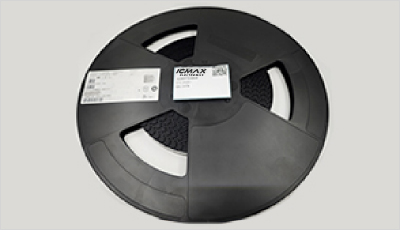
- Step1:Prepare product
-
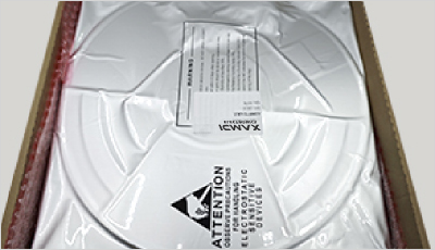
- Step2:Vacuum packaging
-
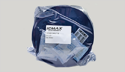
- Step3:Anti-static bag
-
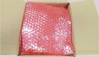
- Step4:Individual package
-
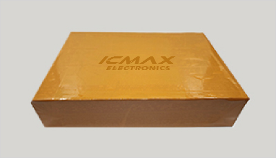
- Step5:Packaging box
-
- Step6:Barcode shipping label
Shipping starts at $40, but some countries will exceed $40. For example (South Africa, Brazil, India, Pakistan, Israel, etc.)
The basic freight (for package ≤0.5kg or corresponding volume) depends on the time zone and country.
Currently, our products are shipped through DHL, FedEx, SF, and UPS.
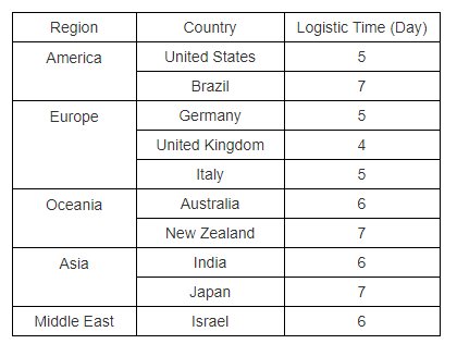
Delivery TimeOnce the goods are shipped, estimated delivery time depends on the shipping methods you chose:
FedEx International, 5-7 business days.
The following are some common countries' logistic time.
- Hot Sale
- Related Categories
- Include Parts
- Popular Search
The following parts include "NCE3010S" in Silicon Labs NCE3010S.
- Part Number
- Manufacturer
- Package
- Description
- BSZ180P03NS3EGATMA1 Infineon Technologies NCE3010S — 30V/10A N-Channel Power MOSFET (SOP-8)The NCE3010S is a 30V/10A trench N-Channel MOSFET in SOP-8 — 12mΩ max at 10V, 16mΩ max at 4.5V, 32.5nC gate charge, from Wuxi NCE Power.From what we see across Shenzhen lots (2025&nda…
- SIRA14DP-T1-GE3 Vishay Siliconix NCE3010S — 30V/10A N-Channel Power MOSFET (SOP-8)The NCE3010S is a 30V/10A trench N-Channel MOSFET in SOP-8 — 12mΩ max at 10V, 16mΩ max at 4.5V, 32.5nC gate charge, from Wuxi NCE Power.From what we see across Shenzhen lots (2025&nda…
- AO4419 Alpha & Omega Semiconductor Inc. NCE3010S — 30V/10A N-Channel Power MOSFET (SOP-8)The NCE3010S is a 30V/10A trench N-Channel MOSFET in SOP-8 — 12mΩ max at 10V, 16mΩ max at 4.5V, 32.5nC gate charge, from Wuxi NCE Power.From what we see across Shenzhen lots (2025&nda…
- SISA14BDN-T1-GE3 Vishay Siliconix NCE3010S — 30V/10A N-Channel Power MOSFET (SOP-8)The NCE3010S is a 30V/10A trench N-Channel MOSFET in SOP-8 — 12mΩ max at 10V, 16mΩ max at 4.5V, 32.5nC gate charge, from Wuxi NCE Power.From what we see across Shenzhen lots (2025&nda…
- PSMN9R5-30YLC,115 Nexperia USA Inc. NCE3010S — 30V/10A N-Channel Power MOSFET (SOP-8)The NCE3010S is a 30V/10A trench N-Channel MOSFET in SOP-8 — 12mΩ max at 10V, 16mΩ max at 4.5V, 32.5nC gate charge, from Wuxi NCE Power.From what we see across Shenzhen lots (2025&nda…
- BUK9Y21-40E,115 Nexperia USA Inc. NCE3010S — 30V/10A N-Channel Power MOSFET (SOP-8)The NCE3010S is a 30V/10A trench N-Channel MOSFET in SOP-8 — 12mΩ max at 10V, 16mΩ max at 4.5V, 32.5nC gate charge, from Wuxi NCE Power.From what we see across Shenzhen lots (2025&nda…
- RTQ035N03HZGTR Rohm Semiconductor NCE3010S — 30V/10A N-Channel Power MOSFET (SOP-8)The NCE3010S is a 30V/10A trench N-Channel MOSFET in SOP-8 — 12mΩ max at 10V, 16mΩ max at 4.5V, 32.5nC gate charge, from Wuxi NCE Power.From what we see across Shenzhen lots (2025&nda…
- FDMS7680 onsemi NCE3010S — 30V/10A N-Channel Power MOSFET (SOP-8)The NCE3010S is a 30V/10A trench N-Channel MOSFET in SOP-8 — 12mΩ max at 10V, 16mΩ max at 4.5V, 32.5nC gate charge, from Wuxi NCE Power.From what we see across Shenzhen lots (2025&nda…
- RQ3E180BNTB Rohm Semiconductor NCE3010S — 30V/10A N-Channel Power MOSFET (SOP-8)The NCE3010S is a 30V/10A trench N-Channel MOSFET in SOP-8 — 12mΩ max at 10V, 16mΩ max at 4.5V, 32.5nC gate charge, from Wuxi NCE Power.From what we see across Shenzhen lots (2025&nda…
- STL6N2VH5 STMicroelectronics NCE3010S — 30V/10A N-Channel Power MOSFET (SOP-8)The NCE3010S is a 30V/10A trench N-Channel MOSFET in SOP-8 — 12mΩ max at 10V, 16mΩ max at 4.5V, 32.5nC gate charge, from Wuxi NCE Power.From what we see across Shenzhen lots (2025&nda…
The following parts are popular search parts in Test and Measurement.
Inventory:50,000
Please send an inquiry. Send us your inquiry, and we will respond immediately.

- 1500+ Daily average RFQ Volume

- 20,000.000 Standard Product Unit

- 1800+ Worldwide Manufacturers

- 15,000+ In-stock Warehouse


