NCE2304 Equivalent, Alternative & Replacement Guide
The NCE2304 is a 30V, 3.6A N-channel MOSFET from Wuxi NCE Power in a SOT-23 package, datasheet v1.0. It publishes on-resistance twice: 58mΩ max at a 10V gate and 73mΩ max at 4.5V.
It gets replaced for one of three reasons — the design needs more current, the gate drive cannot reach 4.5V, or the reel runs dry.
Two parts answer all three and both sit in the same footprint. The AO3400A is the AOS part that defined this slot. The NCE3400 is the same manufacturer's step up.
The deciding specification is not the current rating. It is the gate window, and this is the one place the NCE2304 wins.
This part publishes ±20V. Both alternatives publish ±12V, and that difference decides which designs can use them.
NCE2304 vs AO3400A vs NCE3400: Full Comparison
| Parameter | NCE2304 | AO3400A | NCE3400 |
|---|---|---|---|
| Gate-source maximum (VGS) | ±20V | ±12V | ±12V |
| Gate threshold, min / typ / max | 1.2V / 1.5V / 2.2V | 0.65V / 1.05V / 1.45V | 0.7V / 0.9V / 1.4V |
| RDS(on) max at 10V gate | 58mΩ | 26.5mΩ | 41mΩ |
| RDS(on) max at 4.5V gate | 73mΩ | 32mΩ | 45mΩ |
| RDS(on) max at 2.5V gate | not published | 48mΩ | 45mΩ |
| Continuous current at 25°C | 3.6A | 5.7A | 5.8A |
| Continuous current at 70°C | not published | 4.7A | not published |
| Pulsed current | 15A | 30A | 30A |
| Body diode continuous current | 1.6A | 2A | 2.9A |
| Power dissipation at 25°C | 1.7W | 1.4W | 1.4W |
| Thermal resistance, junction to ambient | 73.5°C/W (10 sec) | 70 typ / 90 max (10 sec); 100 / 125 steady state | prints 1.0°C/W — see note |
| Input capacitance (Ciss) | 230pF | 630pF | 623pF |
| Total gate charge | 4.0nC at 10V | 7nC at 4.5V | 9.5nC at 4.5V |
| Rise / fall time (typ) | 50 / 20 ns | 2.5 / 4 ns | 4.8 / 4 ns |
| Drain-source voltage | 30V on all three | ||
| Package and pinout | SOT-23 — pin 1 gate, pin 2 source, pin 3 drain, on all three | ||
| Junction temperature range | −55°C to 150°C on all three | ||
Read the first row before the rest. The NCE2304 tolerates 20V of gate swing where both alternatives stop at 12V, and that is a real, published difference rather than a rounding one.
The trade is visible two rows down. A wider gate window comes with a thicker gate oxide, and a thicker oxide needs more voltage to reach the same channel. That is why this part's threshold tops out at 2.2V while the other two stop near 1.4V.
At 4.5V of gate drive the span is more than two to one. All three publish a row at that drive, which makes it the one fair comparison point in the group.
None of that makes the NCE2304 a worse part. It makes it the part you pick when the gate rail is the problem, not the load.
When to Use AO3400A
When you need the lowest conduction loss in this footprint. It publishes 26.5mΩ maximum at 10V and 32mΩ at 4.5V, both well below the NCE2304, and its 1.45V maximum threshold means a 3.3V rail turns it on with margin.
When to Use NCE3400
When you need more current and a heavier body diode. It carries 5.8A against 3.6A, and its diode is rated 2.9A against this part's 1.6A — the largest in the group.
It keeps the same pinout, so the swap is a reflow operation.
When NOT to Swap at All
When the existing part is not the problem. A hot NCE2304 is usually copper, not silicon. Check the drain pad area, the via count under it, and the actual ambient inside the enclosure before changing the device.
What Actually Changes When You Swap
The gate window is the only thing that can make a swap illegal. Everything else in that table is a performance difference you can weigh; a 20V-rated gate driven from a 20V rail is a part that dies.
Drawn to scale, the gap is 8V on each rail. A design that lets the gate ring to 15V past the source works on the NCE2304 and does not work on either alternative without a clamp.
That is the whole case for keeping this part in a design that already has one.
The other changes are ordinary. Conduction loss drops on both alternatives, most sharply on the AO3400A. Switching is faster on both, though the gate charge figures are published to different endpoints and should not be compared directly.
What does not change is the footprint. All three use pin 1 gate, pin 2 source, pin 3 drain.
Pinout & Layout Notes
The footprint is identical, so the layout question does not arise. What does arise is the gate drive, because that is the one parameter a reflow cannot change.
Two layout details carry over from the product page. The drain pad is the thermal path, and the 73.5°C/W figure assumes it is soldered to adequate copper. And the source return should be short — it carries the gate loop as well as the load.
Other Alternatives Worth Knowing
Second sources exist, and the threshold is where they diverge. Pin-compatible parts for this slot are sold by other manufacturers, and the published on-resistance usually matches.
The threshold does not. A documented case on the Si2302 shows the genuine part published at a 0.85V maximum while widely available equivalents sat between 1.0V and 1.5V — same part number, different switching point.
Verify the threshold and the gate window against the original sheet before a substitute goes on a production board. Those two rows decide whether the circuit turns on, and neither one travels with the part number.
Lower-voltage parts are not drop-ins. The NCE2312 and NCE2302 are 20V class with the same pinout, and both publish lower on-resistance than the NCE2304 at a 4.5V gate. On a 24V rail they are under-rated, and no amount of pin compatibility fixes that.
A higher-voltage part in the same family is the safe step up. The NCE3400 keeps the 30V rating, the footprint and the pinout, and doubles the current. If the rail is stable, it is the least disruptive upgrade in this group.
Frequently Asked Questions
Q1: Can I drop an AO3400A into an NCE2304 socket?
A: Mechanically yes — the footprint and pinout are identical. Electrically, check the gate rail first. The AO3400A publishes a ±12V gate maximum against this part's ±20V. If the gate can ring near 20V, the substitute dies where the original survived.
Q2: Which alternative has the lowest on-resistance?
A: The AO3400A, at 26.5mΩ maximum at 10V and 32mΩ at 4.5V. The NCE3400 is next at 41mΩ and 45mΩ, and the NCE2304 is highest at 58mΩ and 73mΩ. All three figures are guaranteed maxima at stated test currents.
Q3: Why does the NCE2304 have a wider gate window than the others?
A: A thicker gate oxide, which is also why its threshold is higher. The NCE2304 publishes a 2.2V maximum threshold against roughly 1.4V for both alternatives. The wider window is bought with turn-on headroom, and neither comes free.
Q4: My gate driver only reaches 3.3V. Which part should I use?
A: Either alternative, not the NCE2304. This part publishes on-resistance only at 4.5V and 10V, so 3.3V sits in an uncharacterized region. The AO3400A and NCE3400 both publish rows at lower drive, and both have thresholds that a 3.3V rail clears with margin.
Q5: Do I need a new layout when I swap?
A: No — all three use SOT-23 with pin 1 gate, pin 2 source and pin 3 drain. The swap is a reflow operation. What you should re-check is the copper under the drain pad, because a part rated for more current will not deliver it on the original part's copper.
Q6: Can I compare the gate charge figures directly?
A: No — the three are published to different gate endpoints. The NCE2304 is measured to 10V, the AO3400A and NCE3400 to 4.5V. Gate charge scales with the swing, so the numbers describe test conditions before they describe silicon. Use input capacitance for a cross-part figure.
Q7: Which part has the strongest body diode?
A: The NCE3400 at 2.9A, against 2A for the AO3400A and 1.6A for the NCE2304. All three ratings carry the ten-second qualifier behind the power row. For an inductive load above about 1.5A, the NCE2304's diode is the limiting part of the circuit.
Q8: The NCE3400 datasheet lists a thermal resistance that looks wrong. What happened?
A: It prints 1.0°C/W, which its own dissipation row contradicts. A 1.4W rating against a 150°C junction implies roughly 89°C/W at a 25°C ambient. Work from the dissipation row, or measure the board, rather than trusting that thermal figure.
Q9: Is a substitute part with the same number the same part?
A: Not necessarily, and the threshold is where they differ. Published cases show genuine parts and pin-compatible equivalents with the same number but switching points up to 0.5V apart. Match the threshold and the gate window against the original sheet, not the headline on-resistance.
Q10: Which datasheet revisions do these numbers come from?
A: NCE2304 v1.0 and NCE3400 v1.0 from Wuxi NCE Power, and AO3400A Rev 3.1 from Alpha & Omega Semiconductor. Cross-reference databases often carry rounded figures or present typical values as guaranteed maxima. Where a listing disagrees with the revisioned PDF, the PDF wins.
Related information

-
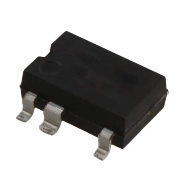
LNK304DN-TL Power Integrations
-
LNK304GN-TL Power Integrations
-
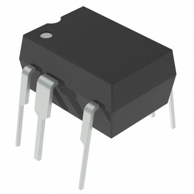
LNK304DG-TL Power Integrations
-
TNY277PN Power Integrations
-
TNY276PN Power Integrations
-
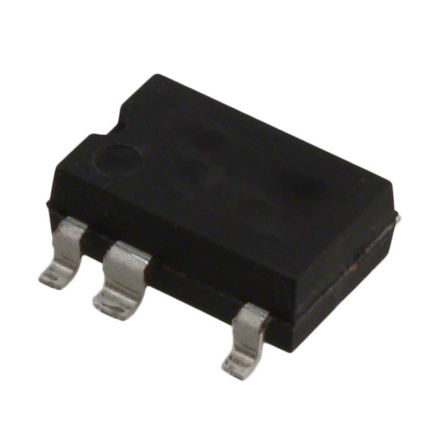
TNY278PN Power Integrations
-
TNY278GN-TL Power Integrations
-
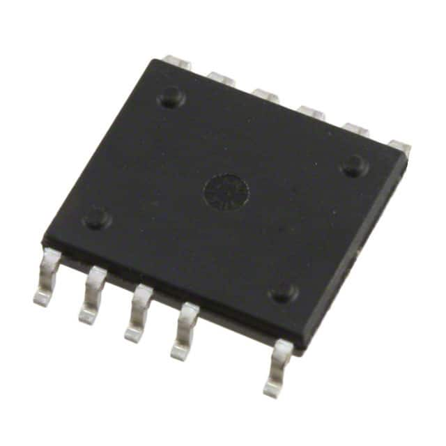
TNY280GN-TL Power Integrations
-
TOP266KG-TL Power Integrations
-
TOP258PN Power Integrations
-
TOP253PN Power Integrations
-
TOP253PNAU Power Integrations

- 1500+ Daily average RFQ Volume

- 20,000.000 Standard Product Unit

- 1800+ Worldwide Manufacturers

- 15,000+ In-stock Warehouse