


Texas Instruments SN74LVC1G07DBVR

- Part No.:
- SN74LVC1G07DBVR
- Manufacturer:
- Texas Instruments
- Package:
- SC-74A, SOT-753
- Datasheet:
-
 SN74LVC1G07DBVR.pdf
- Description:
- IC BUF NON-INVERT 5.5V SOT23-5
- Quantity:
-
Unit Price:$0
Ext Price:$0
- Payment:
-

- Shipping:
-


SN74LVC1G07DBVR Information
- Specifications
- Product Details
- Comparison
- Tags
- Product attributes
- Attribute value
- Manufacturer:
- Texas Instruments
- Series:
- 74LVC
- Package/Case:
- SC-74A, SOT-753
- Packaging:
- Tape & Reel (TR)
- Product Status:
- Active
- Logic Type:
- Buffer, Non-Inverting
- Number of Elements:
- 1
- Number of Bits per Element:
- 1
- Input Type:
- -
- Output Type:
- Open Drain
- Current - Output High, Low:
- -, 32mA
- Voltage - Supply:
- 1.65V ~ 5.5V
- Operating Temperature:
- -40°C ~ 125°C (TA)
- Grade:
- -
- Qualification:
- -
- Mounting Type:
- Surface Mount
- Supplier Device Package:
- SOT-23-5
- Datasheet:
-
SN74LVC1G07DBVR.pdf
SN74LVC245APWR — Octal Bus Transceiver with 3-State Outputs from Texas Instruments
The SN74LVC245APWR is an 8-bit non-inverting bus transceiver from Texas Instruments' 74LVC logic family. It buffers bidirectional data between two buses with 3-state outputs, runs from 1.65V to 3.6V, and tolerates 5V on its inputs — so you can connect a 3.3V microcontroller straight to a legacy 5V peripheral without level shifters.
From what we see in Shenzhen distribution, the LVC245 is one of those parts engineers reach for without thinking — it's the default octal buffer for 3.3V designs. TI has shipped hundreds of millions of them. The TSSOP-20 package is the industry standard footprint, and the pinout is second-sourced by at least four manufacturers.
It's not a glamorous part. It doesn't have a GUI or a register map. But if you've ever needed to isolate a bus, boost a weak GPIO, or bridge two voltage domains with one chip, you know exactly why this part exists.
What Is SN74LVC245APWR and How Does It Work?
The SN74LVC245APWR is an octal bus transceiver — eight bidirectional channels in one TSSOP-20 package. Each channel can pass data in either direction, controlled by a single DIR pin. An OE (Output Enable) pin puts all eight outputs into high-impedance mode, which electrically disconnects the bus.
Think of it as eight controllable doors between two buses. DIR decides which way the doors swing. OE locks them all shut so another device can take over the bus without fighting.
The key number: propagation delay is 6.3 ns max at 3.3V with a 50pF load. Typical is closer to 3.8 ns. At 3.3V, that means it can handle bus speeds well above 100 Mbps before timing becomes the bottleneck.
The "LVC" in the name tells you the silicon story. LVC = Low-Voltage CMOS, TI's family optimized for 3.3V operation with 5V-tolerant inputs. Compared to the older HC family (which needs 5V), LVC gives you faster edges, lower power, and the ability to interface with both old and new logic levels from a single 3.3V rail.
Per the TI datasheet (Rev Q, SCAS293Q), the device also supports partial-power-down operation via Ioff — when VCC is 0V, the outputs stay high-impedance. This is what makes hot-swap and live insertion possible.
What Are the Specifications of SN74LVC245APWR?
| Parameter | Value | Notes |
|---|---|---|
| Manufacturer | Texas Instruments | 74LVC family |
| Function | Octal Bus Transceiver, Non-Inverting | 8 channels |
| Output Type | 3-State | High-impedance when OE = high |
| Supply Voltage (VCC) | 1.65V to 3.6V | Single rail |
| Input Voltage Tolerance | Up to 5.5V | 5V-tolerant on all inputs |
| Max Output Current | ±24 mA per channel | Source and sink |
| Quiescent Current (Iq) | 30 μA max | Near-zero when idle |
| Propagation Delay (tpd) | 6.3 ns max @ 3.3V, 50pF | 3.8 ns typ |
| Output Enable Time | 7.1 ns max @ 3.3V | From OE to output active |
| Input Transition Rate | 10 ns/V max | For clean switching |
| Ioff Partial Power Down | Yes | Outputs high-Z when VCC = 0V |
| ESD Protection | 2000V HBM, 1000V CDM | Per JESD 22 |
| Latch-Up Performance | >250 mA | Per JESD 17 |
| Ground Bounce (VOLP) | <0.8V typ @ 3.3V | Low-noise switching |
| Package | TSSOP-20 (PW) | 6.5 × 4.4 × 1.15 mm |
| Pin Count | 20 | 0.65 mm pitch |
| Operating Temperature | -40°C to +125°C | Industrial range |
| Device Marking | LC245A | Top-side laser mark |
| Packaging | Tape & Reel, 2000 units/reel | 330 mm reel diameter |
Key Numbers That Matter
- tpd = 6.3 ns max at 3.3V (50pF load): This is the number that limits your bus speed. With 6.3 ns of propagation delay, you can comfortably run at 50–100 Mbps depending on setup/hold margins. If your bus is faster than that, you need to check timing — the LVC family is quick but it's not a modern SerDes.
- 5V-tolerant inputs: This is the feature that keeps the LVC245 in BOMs. Your FPGA runs at 3.3V (or even 2.5V), but your peripheral still talks 5V TTL. The LVC245 sits in between and handles the voltage translation without a dedicated level shifter. Just power VCC at 3.3V and connect the 5V signals to the inputs — the device absorbs the overvoltage safely.
- Iq = 30 μA max: In a world where every microamp gets audited, 30 μA is practically free. You can leave this part powered in a battery-operated design and the quiescent draw won't move the needle on battery life.
- Ioff partial-power-down: When VCC is off, the outputs go high-impedance and don't back-drive the bus. Per the TI datasheet (Rev Q), this is tested and guaranteed — it's not a "typical" number. For hot-swap backplanes and live-insertion systems, this is mandatory, not optional.
When Should You Use (and NOT Use) SN74LVC245APWR?
✔ Use SN74LVC245APWR when:
- You need bidirectional 8-bit buffering at 3.3V. This is the canonical use case. MCU on side A, peripheral bus on side B, DIR pin toggled by a GPIO. Done.
- You're bridging 5V and 3.3V domains. The 5V-tolerant inputs make this a one-chip voltage translation solution when your VCC is 3.3V and your input signals come from 5V logic.
- You need bus isolation in a multi-master system. Pull OE high and the device electrically disappears from the bus — all eight outputs go high-Z. No bus contention, no back-drive.
- Your design does hot-swap or live insertion. Ioff guarantees the outputs stay high-impedance with VCC at 0V. This is the feature that separates "might work" from "guaranteed to work" in a hot-plug backplane.
✘ Don't use SN74LVC245APWR when:
- You need direction-sensing (auto-direction). The LVC245 needs a DIR pin — you have to tell it which way data flows. If your bus protocol dynamically changes direction (like I2C or MDIO), you need an automatic bidirectional translator like the TXB0108 or LSF0108 instead.
- You're running below 1.65V. The LVC family bottoms out at 1.65V. For 1.2V or 0.9V logic, look at the AVC (Advanced Very-low-voltage CMOS) family — SN74AVC245 or similar.
- You need registered outputs (latched data). The LVC245 is a transparent buffer — what goes in comes out 4 ns later, but there's no clock, no latch, no storage. For clocked bus holding, use an SN74LVC574 (octal D-type flip-flop) or SN74LVC373 (transparent latch).
- Your bus exceeds 100 Mbps and timing is tight. At 100 Mbps, the bit period is 10 ns. With tpd = 6.3 ns max, you're consuming over 60% of the bit period in propagation delay alone. For faster buses, you need a specialized redriver or a zero-delay buffer like the SN65LVDS series.
What Are the Alternatives to SN74LVC245APWR?
| Parameter | SN74LVC245APWR | SN74LVCH245APWR | 74LCX245MTCX | SN74LVC245ADWR |
|---|---|---|---|---|
| Manufacturer | TI | TI | onsemi | TI |
| Family | LVC | LVCH | LCX | LVC |
| VCC Range | 1.65–3.6V | 1.65–3.6V | 2.0–3.6V | 1.65–3.6V |
| 5V-Tolerant Inputs | Yes | Yes | Yes | Yes |
| Bus Hold | No | Yes | No | No |
| tpd max | 6.3 ns | 7.0 ns | 6.5 ns | 6.3 ns |
| Iout | ±24 mA | ±24 mA | ±24 mA | ±24 mA |
| Package | TSSOP-20 | TSSOP-20 | TSSOP-20 | SOIC-20 |
| Ioff | Yes | Yes | Yes | Yes |
Pick SN74LVCH245APWR when: You need the bus-hold feature — the LVCH variant has internal feedback that holds the last valid logic level on floating inputs. This saves you from pull-up/pull-down resistors on every unused input. In Shenzhen distribution, the LVCH typically runs 10–15% more than the base LVC, but that's cheaper than eight resistors plus placement cost.
Pick 74LCX245MTCX when: You're second-sourcing and want a different manufacturer. The onsemi LCX family is functionally identical — same pinout, same TSSOP-20 package, same voltage range except the low end is 2.0V instead of 1.65V. From our distribution data (2025–2026), LCX parts from onsemi have solid availability and pricing competitive with TI LVC.
Pick SN74LVC245ADWR when: You prefer the SOIC-20 package for hand-soldering or visual inspection. Same die, same specs, wider body (7.5 mm vs 4.4 mm). The DWR variant is the go-to for prototyping and low-volume production where TSSOP's 0.65 mm pitch is more trouble than it's worth.
Pricing & Availability
| Parameter | Details |
|---|---|
| Part Number | SN74LVC245APWR |
| Manufacturer | Texas Instruments |
| Package | TSSOP-20 (PW) |
| Condition | New, original TI |
| Lead Time | In stock, ship from Shenzhen |
| Packing | Tape & Reel (2000 units/reel) |
Contact ICMASS for current pricing. Volume pricing for this part is competitive — it's a high-volume commodity logic IC, and we stock it with full traceability back to TI. For prototyping quantities, we can supply cut-tape or partial reels. Pin-compatible alternatives (SN74LVCH245APWR, 74LCX245MTCX) also available for multi-sourcing if needed.
What Are the Typical Applications of SN74LVC245APWR?
Microcontroller Bus Buffering
The most common scenario: an MCU with 8-bit parallel I/O driving a peripheral bus. The MCU's GPIOs might only source 4–8 mA — the LVC245 boosts that to 24 mA per line while adding less than 4 ns of delay. Per the TI datasheet (Rev Q), all eight channels switch simultaneously with ground bounce under 0.8V.
FPGA-to-Peripheral Level Translation
FPGAs running at 3.3V or 2.5V talk to 5V ADCs, DACs, or display controllers through a single LVC245. No need for a dedicated level translator IC — the 5V-tolerant inputs handle the down-translation. (The LVC245 only translates down — 5V in, 3.3V out. For up-translation, you need a part with a higher VCC or a dedicated level shifter.)
Shared Bus Arbitration
In systems where multiple masters share a data bus, each master's bus lines go through an LVC245. When a master isn't talking, its OE pin is driven high, putting its outputs in high-Z. The active master drives the bus without contention. This is standard practice in telecom line cards and industrial backplanes.
Hot-Swap Backplane Buffering
The Ioff feature guarantees no back-drive when VCC is removed. In a live-insertion system, a card can be plugged in while the backplane is powered — the LVC245's outputs stay high-impedance until the card's VCC ramps up. Per TI characterization, this is tested per JESD 76 (live insertion).
Signal Integrity Cleanup
Weak or noisy signals entering a PCB get cleaned up by the LVC245's Schmitt-trigger-like input structure. The output edges are sharp and symmetric — typically <2 ns rise/fall time at 3.3V. For long traces or ribbon cables, this re-driving action prevents signal degradation from accumulating across connectors.
Frequently Asked Questions About SN74LVC245APWR
Q1: Can SN74LVC245APWR translate 5V signals to 3.3V?
A: Yes — this is the most common use case. Power VCC at 3.3V and connect your 5V signals to the A or B inputs. The 5V-tolerant inputs safely accept the higher voltage, and the outputs swing 0–3.3V. You get 5V-to-3.3V down-translation on all eight channels with no external components. For up-translation (3.3V to 5V), you need a part with 5V VCC like the SN74HCT245.
Q2: How fast can SN74LVC245APWR run?
A: The propagation delay is 6.3 ns max at 3.3V with a 50pF load (3.8 ns typical). That translates to roughly 50–80 Mbps in practice — the bit period at 100 Mbps is 10 ns, so 6.3 ns of tpd leaves only 3.7 ns for setup/hold. Per the TI datasheet (Rev Q, SCAS293Q), faster operation is possible with lighter capacitive loads and higher VCC (closer to 3.6V).
Q3: What is the difference between SN74LVC245A and SN74LVCH245A?
A: The LVCH version adds "bus hold" — internal feedback circuits on the data inputs that hold the last valid logic level when the input goes high-impedance. This eliminates the need for external pull-up or pull-down resistors on unused or floating inputs. The trade-off: LVCH has slightly higher propagation delay (7.0 ns vs 6.3 ns max) and higher input capacitance. From what we see in distribution, most 3.3V designs stick with the base LVC unless floating inputs are a known problem.
Q4: Can I use SN74LVC245APWR with 1.8V logic?
A: Yes — the VCC range goes down to 1.65V, which covers both 1.8V and 2.5V systems. At 1.8V, the propagation delay increases (check the datasheet for exact numbers — it's roughly 2× the 3.3V value) and the output drive drops, but the device is fully functional. Per the TI datasheet (Rev Q), all specs are characterized at 1.8V ±0.15V, 2.5V ±0.2V, 2.7V–3.6V.
Q5: What is the difference between DIR and OE pins?
A: DIR (direction) controls which way data flows — high = A to B, low = B to A. OE (output enable) controls whether the outputs are active or high-impedance — high = all outputs disabled (high-Z), low = outputs active. The two pins are independent. If you set OE high and toggle DIR, nothing happens on the outputs because they're all disabled. If you set OE low and toggle DIR, data reverses direction immediately (within the propagation delay). A common mistake: toggling DIR while OE is low and both buses are driving — this causes momentary bus contention. The safe sequence: OE high first → change DIR → OE low.
Q6: Does SN74LVC245APWR need decoupling capacitors?
A: Yes — standard practice is a 0.1 µF ceramic capacitor as close to the VCC pin as possible. The LVC245 switches eight outputs simultaneously, and the ground bounce spec (<0.8V typ) assumes proper decoupling. Per TI application notes, add a 1–10 µF bulk capacitor nearby if multiple LVC devices share the same VCC rail.
Q7: Is SN74LVC245APWR pin-compatible with 74HC245?
A: Yes, the pinout is identical — both are industry-standard 20-pin octal bus transceivers with DIR at pin 1 and OE at pin 19. But the voltage ranges are completely different. The 74HC245 runs at 2–6V and is designed for 5V systems. The LVC245 runs at 1.65–3.6V. If you put an LVC245 in a 5V-only board, you will exceed its absolute maximum VCC and destroy the part. Always check the supply voltage before cross-referencing logic families.
Q8: Can I leave unused inputs floating?
A: No. Floating CMOS inputs can drift to mid-rail voltages and cause both the P-channel and N-channel transistors to partially conduct — this increases supply current dramatically (milliamps instead of microamps) and can cause oscillation. Tie all unused inputs to GND or VCC through a 10k resistor. For the LVC245 specifically, unused data inputs (A1–A8 or B1–B8) should be tied off. The DIR and OE pins must always be driven — never float the control pins.
Q9: What ESD protection does SN74LVC245APWR have?
A: Per TI's qualification data, the device is rated for 2000V HBM (Human Body Model) and 1000V CDM (Charged Device Model) per JESD 22. This is standard for commercial-grade logic ICs. In production, the device passes JEDEC latch-up testing at >250 mA. For applications with higher ESD requirements (hot-plug front panels, external connectors), add external TVS diodes on the bus lines.
Q10: How many SN74LVC245APWR can I put on one bus?
A: Per the TI datasheet (Rev Q), each output has a fan-out capability determined by the 24 mA drive strength and the input capacitance of downstream devices. In practice, you can typically connect 10–15 LVC inputs to one LVC245 output before rise/fall times degrade beyond spec. The real limit is total bus capacitance — stay under 50pF per output for the specified tpd. For heavily loaded buses (backplanes, multi-card systems), use one LVC245 per card as a bus isolator rather than trying to drive everything from one device.
| Image |

|
|
|
| Part Number | SN74LVC1G07DBVR | SN74LVC1G07DBVRG4 | SN74LVC1G07DBVRE4 |
| Manufacturer | Texas Instruments | Texas Instruments | Texas Instruments |
| Series | 74LVC | 74LVC | 74LVC |
| Package/Case | SC-74A, SOT-753 | SC-74A, SOT-753 | SC-74A, SOT-753 |
| Packaging | Tape & Reel (TR) | Tape & Reel (TR) | Tape & Reel (TR) |
| Product Status | Active | Discontinued at Digi-Key | Discontinued at Digi-Key |
| Logic Type | Buffer, Non-Inverting | Buffer, Non-Inverting | Buffer, Non-Inverting |
| Number of Elements | 1 | 1 | 1 |
| Number of Bits per Element | 1 | 1 | 1 |
| Input Type | - | - | - |
| Output Type | Open Drain | Open Drain | Open Drain |
| Current - Output High, Low | -, 32mA | -, 32mA | -, 32mA |
| Voltage - Supply | 1.65V ~ 5.5V | 1.65V ~ 5.5V | 1.65V ~ 5.5V |
| Operating Temperature | -40°C ~ 125°C (TA) | -40°C ~ 125°C (TA) | -40°C ~ 125°C (TA) |
| Grade | - | - | - |
| Qualification | - | - | - |
| Mounting Type | Surface Mount | Surface Mount | Surface Mount |
| Supplier Device Package | SOT-23-5 | SOT-23-5 | SOT-23-5 |
User Guide
- Purchase & Inquiry
- Package
- Shipping Information
- Customer Review
You may place an order without registering to IC-MAX.COM
We strongly suggest you sign in before purchasing as you can track your order in real time.
For your convenience, we accept multiple payment methods in USD, including PayPal, Credit Card, and wire transfer.
RFQ (Request for Quotations)
It is recommended to request for quotations to get the latest prices and inventories about the part.
Our sales will reply to your request by email within 24 hours.
1. You'll receive an order information email in your inbox. (Please remember to check the spam folder if you didn't hear from us).
2. Since inventories and prices may fluctuate to some extent, the sales manager is going to reconfirm the order and let you know if there are any updates.
-
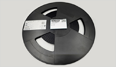
- Step1:Prepare product
-
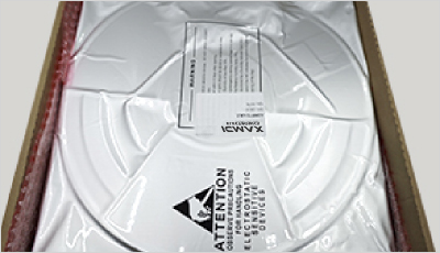
- Step2:Vacuum packaging
-
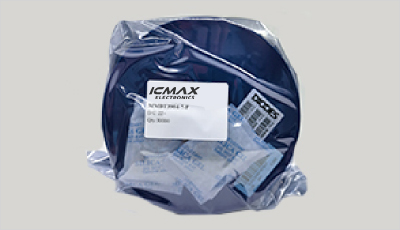
- Step3:Anti-static bag
-
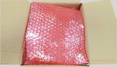
- Step4:Individual package
-
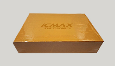
- Step5:Packaging box
-
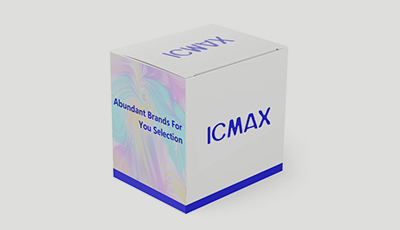
- Step6:Barcode shipping label
Shipping starts at $40, but some countries will exceed $40. For example (South Africa, Brazil, India, Pakistan, Israel, etc.)
The basic freight (for package ≤0.5kg or corresponding volume) depends on the time zone and country.
Currently, our products are shipped through DHL, FedEx, SF, and UPS.
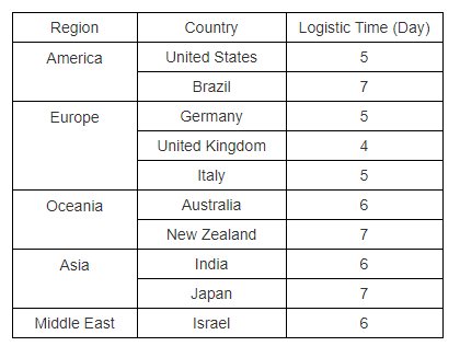
Delivery TimeOnce the goods are shipped, estimated delivery time depends on the shipping methods you chose:
FedEx International, 5-7 business days.
The following are some common countries' logistic time.
- Hot Sale
- Related Categories
- Include Parts
- Popular Search
- Universal Bus Functions(478)
- Translators, Level Shifters(2682)
- Specialty Logic(1247)
- Signal Switches, Multiplexers, Decoders(7433)
- Shift Registers(2074)
- Parity Generators and Checkers(194)
- Multivibrators(655)
- Latches(2949)
- Gates and Inverters - Multi-Function, Configurable(1137)
- Gates and Inverters(13350)
The following parts include "SN74LVC1G07DBVR" in Silicon Labs SN74LVC1G07DBVR.
- Part Number
- Manufacturer
- Package
- Description
- SN74LVC1G17DBVR Texas Instruments SC-74A, SOT-753 IC BUF NON-INVERT 5.5V SOT23-5
- SN74LVC1G07DCKR Texas Instruments SC-74A, SOT-753 IC BUF NON-INVERT 5.5V SOT23-5
- SN74LVC1G17DCKR Texas Instruments SC-74A, SOT-753 IC BUF NON-INVERT 5.5V SOT23-5
- SN74LVC1G07DBVR Texas Instruments SC-74A, SOT-753 IC BUF NON-INVERT 5.5V SOT23-5
- SN74LVC1G125DCKR Texas Instruments SC-74A, SOT-753 IC BUF NON-INVERT 5.5V SOT23-5
- SN74AHCT1G126DBVR Texas Instruments SC-74A, SOT-753 IC BUF NON-INVERT 5.5V SOT23-5
- SN74LVC1G125DBVR Texas Instruments SC-74A, SOT-753 IC BUF NON-INVERT 5.5V SOT23-5
- SN74AHCT1G125DBVR Texas Instruments SC-74A, SOT-753 IC BUF NON-INVERT 5.5V SOT23-5
- SN74LVC2G17DBVR Texas Instruments SC-74A, SOT-753 IC BUF NON-INVERT 5.5V SOT23-5
- SN74LVC2G07DCKR Texas Instruments SC-74A, SOT-753 IC BUF NON-INVERT 5.5V SOT23-5
The following parts are popular search parts in Test and Measurement.
Inventory:60,367
Please send an inquiry. Send us your inquiry, and we will respond immediately.

- 1500+ Daily average RFQ Volume

- 20,000.000 Standard Product Unit

- 1800+ Worldwide Manufacturers

- 15,000+ In-stock Warehouse


