


Texas Instruments SN74HC132DR

- Part No.:
- SN74HC132DR
- Manufacturer:
- Texas Instruments
- Category:
- Gates and Inverters
- Package:
- 14-SOIC (0.154", 3.90mm Width)
- Datasheet:
-
 SN74HC132DR.pdf
- Description:
- IC GATE NAND 4CH 2-INP 14SOIC
- Quantity:
-
Unit Price:$0
Ext Price:$0
- Payment:
-

- Shipping:
-


SN74HC132DR Information
- Specifications
- Product Details
- Comparison
- Tags
- Product attributes
- Attribute value
- Manufacturer:
- Texas Instruments
- Series:
- 74HC
- Package/Case:
- 14-SOIC (0.154", 3.90mm Width)
- Packaging:
- Tape & Reel (TR)
- Product Status:
- Active
- Logic Type:
- NAND Gate
- Number of Circuits:
- 4
- Number of Inputs:
- 2
- Features:
- Schmitt Trigger
- Voltage - Supply:
- 2V ~ 6V
- Current - Quiescent (Max):
- 2 µA
- Current - Output High, Low:
- 5.2mA, 5.2mA
- Input Logic Level - Low:
- 0.3V ~ 1.2V
- Input Logic Level - High:
- 1.5V ~ 4.2V
- Max Propagation Delay @ V, Max CL:
- 21ns @ 6V, 50pF
- Operating Temperature:
- -40°C ~ 85°C
- Grade:
- -
- Qualification:
- -
- Mounting Type:
- Surface Mount
- Supplier Device Package:
- 14-SOIC
- Datasheet:
-
SN74HC132DR.pdf
SN74HC132DR — Quad 2-Input NAND Gate with Schmitt-Trigger Inputs from Texas Instruments
The SN74HC132DR is a quad 2-input NAND gate with Schmitt-trigger inputs from Texas Instruments' 74HC logic family — four independent NAND gates in one 14-pin SOIC package. The Schmitt-trigger inputs give each gate hysteresis: the voltage that triggers a LOW→HIGH transition is different from the voltage that triggers HIGH→LOW. This means slow, noisy, or ragged input signals come out clean on the other side.
From what we see in Shenzhen distribution, the HC132 is the part engineers grab when they need to turn a crummy analog signal into a clean digital one without writing firmware. It's the Swiss Army knife of signal conditioning: debounce a switch, build an RC oscillator, clean up a sensor output, or gate a clock — one chip, four gates, done.
What separates it from a standard 74HC00 (quad NAND without Schmitt triggers): if you feed a slow-rising signal to a 74HC00, the output can oscillate as the input crosses the threshold region. The HC132 doesn't do that. The hysteresis band — typically 0.8V at 4.5V VCC per the TI datasheet — acts like a dead zone that the input has to fully cross before the output toggles. No chatter, no glitches.
What Is SN74HC132DR and How Does It Work?
It's a quad 2-input NAND gate. Each of the four gates takes two inputs (A and B) and produces Y = NOT (A AND B). In plain English: if both inputs are HIGH, the output goes LOW. Any other combination → output HIGH.
The Schmitt-trigger part is what makes it special. A normal logic gate has a single input threshold — above it is HIGH, below is LOW. If the input hovers near that threshold (because it's noisy, or slow, or both), the output can flip back and forth rapidly. The HC132 has two thresholds instead of one: a higher threshold for LOW→HIGH transitions (VT+) and a lower threshold for HIGH→LOW transitions (VT-). The gap between them is the hysteresis voltage.
Per the TI datasheet (Rev H, SCLS309H), typical VT+ is 1.6V and VT- is 0.8V at 4.5V VCC — that's 0.8V of hysteresis. An input has to rise above 1.6V to switch the output LOW, and then fall below 0.8V to switch it back HIGH. A 0.5V noise spike in the middle does nothing.
The HC family runs at 2V to 6V, which makes it one of the few logic families that's genuinely happy at both 3.3V and 5V. At 5V, propagation delay is typically 14 ns (25 ns max), pushing well past 30 MHz if you're using it as an oscillator.
What Are the Specifications of SN74HC132DR?
| Parameter | Value | Notes |
|---|---|---|
| Manufacturer | Texas Instruments | 74HC logic family |
| Logic Function | Quad 2-Input NAND | 4 independent gates |
| Schmitt-Trigger Inputs | Yes, on all inputs | Hysteresis on every gate |
| Supply Voltage (VCC) | 2V to 6V | 5V nominal |
| Quiescent Current (ICC) | 2 µA typ, 20 µA max | Near-zero static power |
| Output Drive (IOH/IOL) | ±5.2 mA at 6V | ±4 mA at 4.5V |
| VT+ (positive threshold) | 1.6V typ at 4.5V VCC | Rising input |
| VT- (negative threshold) | 0.8V typ at 4.5V VCC | Falling input |
| Hysteresis (VT+ - VT-) | 0.8V typ at 4.5V VCC | Noise immunity zone |
| Propagation Delay (tpd) | 14 ns typ, 25 ns max | At 4.5V, 50pF |
| Max tpd at 2V | 120 ns | Slower at low voltage |
| Input Capacitance | 3 pF typ | Per input |
| ESD Protection | 2000V HBM, 1000V CDM | Per JESD 22 |
| Package | SOIC-14 (D) | 8.65 × 3.91 × 1.58 mm |
| Pin Count | 14 | 1.27 mm pitch |
| Operating Temperature | -40°C to +85°C | Industrial grade |
| Device Marking | HC132 | Top-side laser mark |
Key Numbers That Matter
- Hysteresis = 0.8V typical at 4.5V VCC: This is the whole reason you buy an HC132 instead of an HC00. If your input signal has 500 mV of noise riding on it, a standard gate will chatter every time the noise crosses the threshold. The HC132's 0.8V hysteresis window swallows that 500 mV of noise completely. The signal has to move a full 0.8V in the opposite direction before the output even considers toggling. Per the TI datasheet (Rev H), the hysteresis is temperature-compensated — it stays consistent from -40°C to +85°C.
- tpd = 14 ns typical (25 ns max) at 4.5V: Fast enough for oscillator circuits into the tens of MHz. In a ring oscillator configuration (one gate feeding the next), you can get oscillation frequencies well above 30 MHz. At 2V, the delay stretches to 120 ns — if you're running at low voltage, account for the speed derating.
- ICC = 2 µA typical: Per the TI datasheet (Rev H, SCLS309H), when inputs are held at valid logic levels, the entire chip draws 2 µA. That's four Schmitt-trigger NAND gates consuming less power than a single pull-up resistor. For battery-powered designs where the HC132 serves as a wake-up monitor or button debouncer, the quiescent draw is invisible.
When Should You Use (and NOT Use) SN74HC132DR?
✔ Use SN74HC132DR when:
- You need to clean up a noisy or slow-rising signal. This is the #1 use case. Sensor output, mechanical switch, long cable run, optocoupler — anything that doesn't produce a clean digital edge. Feed it through an HC132 gate and the output is a crisp square wave.
- You're building an RC relaxation oscillator. One gate, one resistor, one capacitor, and you've got a clock source. The Schmitt hysteresis is what makes it oscillate — the capacitor charges through R until it hits VT+, the output flips, the capacitor discharges to VT-, the output flips back. No crystal, no PLL, just three passives. Frequency ≈ 1/(RC), and it's stable enough for LED blinking, button polling, or a low-speed system clock.
- You need switch debouncing in hardware. Mechanical switches bounce for 1–10 ms. An RC filter + one HC132 gate eliminates the bounce without a line of code. The Schmitt hysteresis ensures the slow RC ramp produces exactly one clean edge.
- You're gating a clock or enable signal that might be glitchy. Two inputs: one is your signal, the other is your gate/enable. If the signal is clean but the enable might have ringing, the Schmitt inputs on both pins prevent false triggers.
✘ Don't use SN74HC132DR when:
- You need 5V-tolerant inputs on a 3.3V system. HC devices are not overvoltage-tolerant — input voltages must not exceed VCC. If you're running at 3.3V and need to accept 5V inputs, use the SN74AHC132 (Advanced HC with 5V-tolerant inputs) or the SN74LV132A (LV family, 5V-tolerant).
- You need sub-10 ns propagation delay. At 14 ns typical, the HC132 is fast for general logic but not fast enough for 100 MHz+ clock distribution. For higher speed, the SN74AC132 (Advanced CMOS) delivers tpd of 5–10 ns.
- You need the CD4093 pinout. The CD4093 is the older 4000-series quad NAND Schmitt trigger with a different pinout (and 3V–15V supply). The HC132 is faster and lower-power at 5V, but it's not pin-compatible with a 4093 socket.
- You need open-drain outputs. The HC132 has push-pull outputs. For wired-OR or level-shifting with pull-up resistors, use an open-drain gate like the SN74HC03 (quad NAND, open-drain) — but note the HC03 doesn't have Schmitt inputs.
What Are the Alternatives to SN74HC132DR?
| Parameter | SN74HC132DR | SN74AC132DR | SN74AHC132DR | CD4093BE |
|---|---|---|---|---|
| Manufacturer | TI | TI | TI | TI |
| Family | HC | AC | AHC | CD4000 |
| VCC Range | 2–6V | 2–6V | 2–5.5V | 3–15V |
| tpd (typ) | 14 ns | 5 ns | 12 ns | 60 ns |
| Hysteresis at 5V | 0.8V | 0.6V | 0.6V | 1.5V |
| 5V-Tolerant Inputs | No | No | Yes | Yes (up to VCC) |
| Output Drive | ±5.2 mA | ±24 mA | ±8 mA | ±2.5 mA |
| Package | SOIC-14 | SOIC-14 | SOIC-14 | DIP-14 |
| Pinout | HC132 | HC132 | HC132 | Different |
| Temp Range | -40 to +85°C | -40 to +85°C | -40 to +125°C | -55 to +125°C |
Pick SN74AC132DR when: Speed is everything. The AC (Advanced CMOS) family cuts tpd to 5 ns typical — nearly 3× faster than HC — and boosts output drive to ±24 mA. If you're building a high-frequency oscillator or driving a long trace, AC is the upgrade. The trade-off: AC devices are slightly more expensive and have higher dynamic power consumption due to faster edges.
Pick SN74AHC132DR when: You're running at 3.3V and need to accept 5V inputs. The AHC family's 5V-tolerant inputs solve the overvoltage problem that standard HC can't handle. From our distribution data (2025–2026), AHC132 availability is solid and pricing is comparable to HC.
Pick CD4093BE when: You're running above 6V (the HC132's ceiling). The CD4093 works from 3V all the way to 15V, making it the go-to for 12V or 15V systems. It's slower (60 ns tpd) and has a different pinout, but the hysteresis is massive — typically 1.5V at 5V, and proportionally larger at higher VCC. For noisy industrial 12V/24V environments, the 4093's huge hysteresis window is a feature, not a bug.
Pricing & Availability
| Parameter | Details |
|---|---|
| Part Number | SN74HC132DR |
| Manufacturer | Texas Instruments |
| Package | SOIC-14 (D) |
| Condition | New, original TI |
| Lead Time | In stock, ship from Shenzhen |
| Packing | Tape & Reel (2500 units/reel) |
Contact ICMASS for current pricing. The HC132 is a commodity logic gate — pricing is competitive at any volume. We stock the SOIC-14 package with full TI traceability. Pin-compatible speed upgrades (SN74AC132DR, SN74AHC132DR) also available if your design needs lower propagation delay or 5V-tolerant inputs.
What Are the Typical Applications of SN74HC132DR?
RC Relaxation Oscillator
One gate, one resistor (R), one capacitor (C), oscillating at roughly f = 1/(RC). Connect the output to one input through a feedback resistor, connect the other input to a capacitor to ground, and tie the second input of the gate HIGH to enable. The HC132's hysteresis makes this self-starting and stable. Per the TI datasheet (Rev H), at 5V the thresholds are VT+ ≈ 1.6V, VT- ≈ 0.8V, giving a predictable charge/discharge window. Frequency tolerance is set mostly by the R and C tolerance — for a 1% resistor and 5% capacitor, expect roughly ±10% on frequency. Good enough for a blinking LED, a low-speed system clock, or a PWM ramp generator.
Hardware Switch Debounce
Mechanical contacts bounce — a button press isn't one clean edge, it's a burst of 10–50 rapid on/off transitions lasting 1–10 ms. The classic fix: an RC low-pass filter (10kΩ pull-up, 0.1 µF to ground = 1 ms time constant) feeding one HC132 gate. The RC smooths the bounce into a slow ramp. The Schmitt hysteresis turns that ramp into exactly one clean edge. No firmware debounce routine, no timer ISR, no missed edges. One gate per button — and you've got four gates per chip.
Sensor Signal Conditioning
Analog sensors (thermistors, photodiodes, Hall-effect switches with analog output) often produce signals that cross a logic threshold slowly or with noise. An HC132 gate set up as a threshold detector: adjust the input voltage divider so the sensor crosses VT+ and VT- at the desired trigger points. The hysteresis provides a built-in deadband — the sensor has to move a meaningful amount before the output changes state, preventing chatter around the trigger point.
Clock Gating with Glitch Removal
Two-input NAND gate: one input is your clock, the other is your enable. If the enable signal has ringing or bounce (from a mechanical switch or long cable), a standard gate would pass every glitch through to the clock output. The HC132's Schmitt inputs on both pins reject the noise on the enable line, producing a clean gated clock. Just be aware: gating a clock this way can produce runt pulses if the enable changes while the clock is HIGH. For synchronous clock gating, use a dedicated clock gate or synchronize the enable to the falling edge first.
Power-On Reset Generator
An RC network on one input (with the capacitor slowly charging from 0V to VCC at power-up) and the other input tied HIGH creates a power-on reset pulse. The output stays HIGH while the capacitor charges through VT+, then goes LOW — the duration is set by R × C × ln(VCC / (VCC - VT+)). With R = 100kΩ and C = 1 µF at 5V, that's roughly 60 ms of active-low reset. Add a discharge diode across R for fast recovery on power-down.
Frequently Asked Questions About SN74HC132DR
Q1: What is the difference between SN74HC132 and SN74HC00?
A: Both are quad 2-input NAND gates with identical pinouts. The difference: the HC132 has Schmitt-trigger inputs on every gate; the HC00 does not. If you feed a slow or noisy signal to an HC00, the output may oscillate as the input crosses the threshold. The HC132's hysteresis (0.8V typ at 5V) prevents this. If your inputs are clean, fast digital signals, the HC00 works fine and is slightly cheaper. If there's any chance of slow edges or noise, use the HC132.
Q2: How do I build an oscillator with SN74HC132?
A: Use one NAND gate. Connect the output to one input through a resistor R. Connect a capacitor C from that input to ground. Tie the second input HIGH to enable oscillation. Frequency ≈ 1/(RC). At 5V, with R = 100kΩ and C = 10 nF, expect roughly 1 kHz. Per the TI datasheet (Rev H), thresholds are temperature-compensated but not trimmed to a precision voltage. For stable frequency, use a crystal oscillator instead.
Q3: Can I run SN74HC132DR at 3.3V?
A: Yes. The HC family operates from 2V to 6V. At 3.3V, tpd increases to ~20–30 ns and hysteresis shrinks to ~0.4–0.6V. Output drive drops to roughly ±2 mA. Per the TI datasheet (Rev H, SCLS309H), all parameters are characterized at 3.3V ±0.3V.
Q4: Are unused gates a problem - do I need to tie them off?
A: Yes, always tie off unused inputs. Floating CMOS inputs drift to mid-rail and cause the gate to draw excess current (milliamps instead of microamps) and potentially oscillate. Tie both inputs of unused gates to GND (output goes HIGH, gate is stable). Never leave inputs floating.
Q5: How does the hysteresis work at different voltages?
A: Per the TI datasheet (Rev H), hysteresis is roughly proportional to VCC. At 2V: ~0.7V hysteresis. At 4.5V: ~0.8V. At 6V: ~1.0V. The thresholds are temperature-compensated over -40°C to +85°C. Don't use the HC132 at 2V if you need the full 0.8V noise immunity.
Q6: Can I use this as a level shifter (3.3V to 5V)?
A: For 3.3V → 5V: Power the HC132 at 5V. A 3.3V HIGH will exceed VT+ (2.7V max at 5V VCC) and be recognized. This works. For 5V → 3.3V: You cannot feed 5V into an HC132 powered at 3.3V. Use the SN74AHC132 (5V-tolerant inputs) or a dedicated level translator.
Q7: What's the maximum frequency I can get from an HC132 oscillator?
A: At 5V, the practical ceiling is 35–40 MHz. With tpd = 14 ns, a full oscillation cycle takes at least ~28 ns (two transitions). Per TI application notes, a reliable range is 1 Hz to 10 MHz. For stable operation above 20 MHz, use the AC family (SN74AC132, tpd 5 ns).
Q8: Can I parallel multiple gates for more drive current?
A: Yes. Tie corresponding inputs together and connect outputs together. Propagation delays match closely enough on the same die that output contention is not a problem. Maximum combined drive from all four gates in parallel: roughly ±20 mA at 5V.
Q9: Is SN74HC132DR a direct replacement for the old 74132?
A: Pinout is identical. Electrical differences: HC runs 2–6V vs TTL 5V ±5%; HC inputs draw nanoamps vs TTL milliamps; HC hysteresis is larger and better-controlled. In most 5V designs, the HC132 is a drop-in upgrade with lower power. If your design relies on TTL input current for pull-down biasing, recalculate resistor values.
Q10: What causes the output to oscillate when it shouldn't?
A: Three common causes. (1) Floating inputs — tie all unused inputs to GND or VCC. (2) No decoupling capacitor — place a 0.1 µF ceramic cap directly across VCC and GND. Fast output edges draw sharp current spikes that can couple into inputs through supply bounce. (3) Slow input edge at low VCC — increase VCC or pre-condition the signal with an RC filter before the gate.
| Image |

|
|
|
| Part Number | SN74HC132DR | SN74HC132DRE4 | SN74HC132DRG4 |
| Manufacturer | Texas Instruments | Texas Instruments | Texas Instruments |
| Series | 74HC | 74HC | 74HC |
| Package/Case | 14-SOIC (0.154", 3.90mm Width) | 14-SOIC (0.154", 3.90mm Width) | 14-SOIC (0.154", 3.90mm Width) |
| Packaging | Tape & Reel (TR) | Tape & Reel (TR) | Tape & Reel (TR) |
| Product Status | Active | Obsolete | Obsolete |
| Logic Type | NAND Gate | NAND Gate | NAND Gate |
| Number of Circuits | 4 | 4 | 4 |
| Number of Inputs | 2 | 2 | 2 |
| Features | Schmitt Trigger | Schmitt Trigger | Schmitt Trigger |
| Voltage - Supply | 2V ~ 6V | 2V ~ 6V | 2V ~ 6V |
| Current - Quiescent (Max) | 2 µA | 2 µA | 2 µA |
| Current - Output High, Low | 5.2mA, 5.2mA | 5.2mA, 5.2mA | 5.2mA, 5.2mA |
| Input Logic Level - Low | 0.3V ~ 1.2V | 0.3V ~ 1.2V | 0.3V ~ 1.2V |
| Input Logic Level - High | 1.5V ~ 4.2V | 1.5V ~ 4.2V | 1.5V ~ 4.2V |
| Max Propagation Delay @ V, Max CL | 21ns @ 6V, 50pF | 21ns @ 6V, 50pF | 21ns @ 6V, 50pF |
| Operating Temperature | -40°C ~ 85°C | -40°C ~ 85°C | -40°C ~ 85°C |
| Grade | - | - | - |
| Qualification | - | - | - |
| Mounting Type | Surface Mount | Surface Mount | Surface Mount |
| Supplier Device Package | 14-SOIC | 14-SOIC | 14-SOIC |
User Guide
- Purchase & Inquiry
- Package
- Shipping Information
- Customer Review
You may place an order without registering to IC-MAX.COM
We strongly suggest you sign in before purchasing as you can track your order in real time.
For your convenience, we accept multiple payment methods in USD, including PayPal, Credit Card, and wire transfer.
RFQ (Request for Quotations)
It is recommended to request for quotations to get the latest prices and inventories about the part.
Our sales will reply to your request by email within 24 hours.
1. You'll receive an order information email in your inbox. (Please remember to check the spam folder if you didn't hear from us).
2. Since inventories and prices may fluctuate to some extent, the sales manager is going to reconfirm the order and let you know if there are any updates.
-
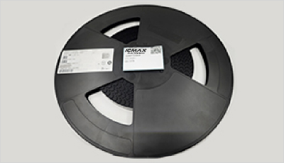
- Step1:Prepare product
-
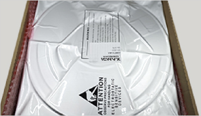
- Step2:Vacuum packaging
-
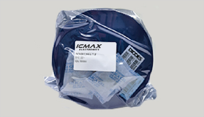
- Step3:Anti-static bag
-
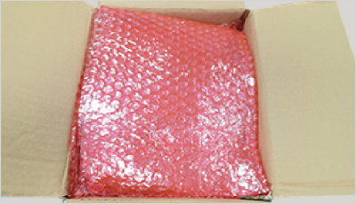
- Step4:Individual package
-
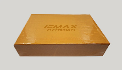
- Step5:Packaging box
-

- Step6:Barcode shipping label
Shipping starts at $40, but some countries will exceed $40. For example (South Africa, Brazil, India, Pakistan, Israel, etc.)
The basic freight (for package ≤0.5kg or corresponding volume) depends on the time zone and country.
Currently, our products are shipped through DHL, FedEx, SF, and UPS.
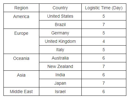
Delivery TimeOnce the goods are shipped, estimated delivery time depends on the shipping methods you chose:
FedEx International, 5-7 business days.
The following are some common countries' logistic time.
- Hot Sale
- Related Categories
- Include Parts
- Popular Search
- Universal Bus Functions(478)
- Translators, Level Shifters(2682)
- Specialty Logic(1247)
- Signal Switches, Multiplexers, Decoders(7433)
- Shift Registers(2074)
- Parity Generators and Checkers(194)
- Multivibrators(655)
- Latches(2949)
- Gates and Inverters - Multi-Function, Configurable(1137)
- Gates and Inverters(13350)
The following parts include "SN74HC132DR" in Silicon Labs SN74HC132DR.
- Part Number
- Manufacturer
- Package
- Description
- SN74LVC1G14DBVR Texas Instruments 14-SOIC (0.154", 3.90mm Width) IC GATE NAND 4CH 2-INP 14SOIC
- SN74LVC1G14DCKR Texas Instruments 14-SOIC (0.154", 3.90mm Width) IC GATE NAND 4CH 2-INP 14SOIC
- SN74AHC1G14DBVR Texas Instruments 14-SOIC (0.154", 3.90mm Width) IC GATE NAND 4CH 2-INP 14SOIC
- SN74LVC1G08DBVR Texas Instruments 14-SOIC (0.154", 3.90mm Width) IC GATE NAND 4CH 2-INP 14SOIC
- SN74LVC1G08DCKR Texas Instruments 14-SOIC (0.154", 3.90mm Width) IC GATE NAND 4CH 2-INP 14SOIC
- SN74LVC1G32DCKR Texas Instruments 14-SOIC (0.154", 3.90mm Width) IC GATE NAND 4CH 2-INP 14SOIC
- SN74LVC1G04DBVR Texas Instruments 14-SOIC (0.154", 3.90mm Width) IC GATE NAND 4CH 2-INP 14SOIC
- 74LVC1G08GW,125 Nexperia USA Inc. 14-SOIC (0.154", 3.90mm Width) IC GATE NAND 4CH 2-INP 14SOIC
- SN74LVC1G04DCKR Texas Instruments 14-SOIC (0.154", 3.90mm Width) IC GATE NAND 4CH 2-INP 14SOIC
- SN74AHC1G08DBVR Texas Instruments 14-SOIC (0.154", 3.90mm Width) IC GATE NAND 4CH 2-INP 14SOIC
The following parts are popular search parts in Test and Measurement.
Inventory:11,500
Please send an inquiry. Send us your inquiry, and we will respond immediately.

- 1500+ Daily average RFQ Volume

- 20,000.000 Standard Product Unit

- 1800+ Worldwide Manufacturers

- 15,000+ In-stock Warehouse


