


onsemi MC74HC4052ADR2G

- Part No.:
- MC74HC4052ADR2G
- Manufacturer:
- onsemi
- Package:
- 16-SOIC (0.154", 3.90mm Width)
- Datasheet:
-
 MC74HC4052ADR2G.pdf
- Description:
- IC SWITCH SP4T X 2 100OHM 16SOIC
- Quantity:
-
Unit Price:$0
Ext Price:$0
- Payment:
-

- Shipping:
-


MC74HC4052ADR2G Information
- Specifications
- Product Details
- Comparison
- Tags
- Product attributes
- Attribute value
- Manufacturer:
- onsemi
- Series:
- -
- Packaging:
- Tape & Reel (TR)
- Product Status:
- Active
- Switch Circuit:
- SP4T
- Multiplexer/Demultiplexer Circuit:
- 4:1
- Number of Circuits:
- 2
- On-State Resistance (Max):
- 100Ohm
- Channel-to-Channel Matching (ΔRon):
- 10Ohm
- Voltage - Supply, Single (V+):
- 2V ~ 6V
- Voltage - Supply, Dual (V±):
- ±2V ~ 6V
- Switch Time (Ton, Toff) (Max):
- -
- -3db Bandwidth:
- 95MHz
- Charge Injection:
- -
- Channel Capacitance (CS(off), CD(off)):
- 80pF
- Current - Leakage (IS(off)) (Max):
- 100nA
- Crosstalk:
- -60dB @ 1MHz
- Operating Temperature:
- -55°C ~ 125°C (TA)
- Grade:
- -
- Qualification:
- -
- Mounting Type:
- Surface Mount
- Supplier Device Package:
- 16-SOIC
- Datasheet:
-
MC74HC4052ADR2G.pdf
MC74HC4052ADR2G — Dual 4-Channel Analog Multiplexer/Demultiplexer with Low Crosstalk (SOP-16)
The MC74HC4052ADR2G is ON Semiconductor's dual 4-channel analog multiplexer/demultiplexer — two independent 4:1 switches that route analog signals, not just digital levels, in one SOP-16.
Two address bits (A, B) steer each of the two switch blocks, and a single enable turns everything off. The analog path runs from VEE to VCC, so it handles bipolar signals — audio, sensor rails, and ADC inputs — with a typical on-resistance around 190Ω.
In the boards we support (2025–2026), the misdiagnosis we see most with this class of part: a circuit's gain drifts, and the engineer swaps the op-amp before discovering the real culprit — the mux's Ron sitting in the feedback path.
It's a switch, not a wire — treat the 190Ω as a design parameter, and it behaves.
What Are the Technical Specifications of MC74HC4052ADR2G?
| Parameter | Value |
|---|---|
| Type | Dual 4-channel analog multiplexer/demultiplexer (2 × 4:1) |
| Analog Supply (VCC − VEE) | 2.0V to 12.0V |
| Digital Supply (VCC − GND) | 2.0V to 6.0V |
| VEE Range | -6.0V to GND |
| On-Resistance (Ron) | ~190Ω typical (2 circuits); ~210Ω @4.5V, ~160Ω @VEE=-4.5V |
| Off Leakage | Low, diode-protected inputs/outputs |
| Select Inputs | A, B (2 bits per switch block) + single ENABLE (high = all switches off) |
| Signal Range | VEE–0.5V to VCC+0.5V (any analog pin) |
| Quiescent Current | 1µA typical |
| Input Leakage | ±0.1µA @25°C |
| Operating Temperature | -55°C to +125°C |
| Package / Pinout | SOP-16: 1=Y0, 2=Y2, 3=Ycom, 4=Y3, 5=Y1, 6=EN, 7=VEE, 8=GND, 9=B, 10=A, 11=X3, 12=Xcom, 13=X0, 14=X1, 15=X2, 16=VCC |
| Chip Complexity | 168 FETs / 42 equivalent gates |
| Compliance | Pb-free, halogen-free, RoHS; NLV prefix = AEC-Q100 automotive |
Key numbers that matter: Per the ON Semiconductor MC74HC4052A datasheet (Rev 8), the analog path spans the full VEE to VCC window — that is what makes this an analog part rather than a digital one. Bipolar audio and negative sensor rails work where a 595 or 138 never could.
The ~190Ω Ron is the number to respect: low enough for signals into high-impedance loads, real enough to corrupt a precision circuit if it ends up in a feedback path.
Read the pinout as two 4:1 switches, not one 8:1: X and Y are independent blocks — audio left and right, or two sensor banks, switched by the same A/B address.
The pin numbering looks scrambled (Y0 at pin 1, Y1 at pin 5) because the two commons sit between their own channels.
When Should You Use (and NOT Use) the MC74HC4052ADR2G?
✅ Use MC74HC4052ADR2G when:
- Routing audio or bipolar signals. With VEE tied to a negative rail, the switch passes signals from -5V to +5V — the 595 and 138 class cannot touch these.
- Multiplexing sensors into one ADC. Four (or eight, with both blocks) analog channels share a single ADC input. Keep the source impedance low and the Ron voltage drop fits the ADC's error budget.
- Gain switching in the inverting input path. Put the mux in series with the op-amp's inverting input — no feedback current flows through Ron, so it causes no gain error.
- 2.0V–12.0V analog rails. The wide VCC–VEE window covers 3.3V audio, 5V sensors, and 12V industrial signal levels.
- Break-before-make channel switching. The family's switching behavior keeps two channels from shorting together during a transition.
❌ Don't use MC74HC4052ADR2G when:
- The circuit needs 1% accuracy from a high-impedance source. The ~190Ω Ron is a voltage divider with your source impedance — for precision acquisition use a low-Ron mux (TMUX1109-class) or buffer first.
- The switch sits in an op-amp feedback loop. Ron in the feedback path changes the gain — a classic EEVblog failure mode where a 1/10/100 gain stage measured 1/1.1/2.16 instead. Move the mux out of the loop.
- Signals may exceed the supply rails. Inputs are diode-clamped to VEE and VCC — an over-range input conducts into the rails and produces crosstalk on every channel.
- You're switching the power path itself. 190Ω cannot carry load current — use a load switch, relay, or the TPIC6B595 for anything that powers something.
What Are the Alternatives to MC74HC4052ADR2G?
| Model | Type | Key Difference | Best For |
|---|---|---|---|
| MC14052B | Dual 4:1 mux, metal gate | Pin-compatible predecessor, higher Ron, older process | Drop-in legacy designs at slower speeds |
| MC74HC4051A | 8:1 mux | Single 8-channel switch, same family and Ron class | Eight channels into one common |
| MC74HC4053A | Triple 2:1 mux | Three independent SPDT switches | Stereo audio switching, differential signals |
| TMUX1109 / TS3A4741 | Precision mux | Ron down to ~1Ω class, injection-current tolerant | Precision measurement, ADC front ends |
| HC4851A / HC4852A | Mux with injection protection | ON's recommended parts when input currents can inject | Industrial inputs that exceed the rails |
Pick by what crosses the switch. General analog routing — the 4052. One rail-limited signal — the 4051. Stereo or differential — the 4053. Precision — TMUX1109-class with Ron under 2Ω. And if over-voltage inputs are a real risk, ON's own datasheet points to the HC485xA family with injection protection.
What Are the Typical Applications of MC74HC4052ADR2G?
Four-Sensor ADC Front End: Four thermistor or sensor channels share one ADC input. Each channel is selected by A/B, the mux output feeds the ADC through a buffer — the buffer's high input impedance makes the 190Ω Ron irrelevant, and one ADC serves four sensors.
Stereo Audio Input Selection: Two 4052 blocks carry left and right channels, so a single A/B address picks one of four stereo sources. With VEE on a -5V rail, line-level audio swings without distortion, and the low crosstalk keeps channel separation clean.
Programmable-Gain Instrumentation: The mux selects feedback resistors in the inverting input path of an op-amp, not the feedback loop itself. Because no feedback current crosses the switch, the gain stays exact — the forum-proven way to use a 4052 in a precision stage.
Why the buffer earns its place: the ADC input impedance is high, but the sensor might be a high-impedance source too — and 190Ω in series with a 10kΩ source is a 2% error. A unity-gain buffer between mux and ADC makes the switch resistance disappear entirely.
Why Buy MC74HC4052ADR2G from ICMASS?
Genuine ON silicon, tested for the family swap. The 4051/4052/4053 trio shares a body but not a topology — we verify channel count and the dual-block routing on incoming lots so the switch you get matches the address map you wrote.
Analog + logic families in one shipment. You're ordering the 4052 for analog routing, the 595 for outputs, and the 138 for decode — we stock the ON and TI families from Shenzhen with same-day dispatch.
Cross-reference support. Not sure whether your front end needs the general 4052, the 8:1 4051, or a precision TMUX-class part? Tell us the signal level, the source impedance, and the accuracy budget — we'll confirm the right switch before you commit the BOM.
Frequently Asked Questions About MC74HC4052ADR2G
Q1: What is the MC74HC4052ADR2G?
A: A dual 4-channel analog multiplexer/demultiplexer — two independent 4:1 switches in one SOP-16. ON Semiconductor's version routes analog signals from VEE to VCC with a typical on-resistance around 190Ω, controlled by two address bits and one enable.
Q2: What is the on-resistance of the 74HC4052?
A: About 190Ω typical — roughly 210Ω at 4.5V, down to 160Ω with a -4.5V VEE. Ron varies with the input signal voltage, which is why precision circuits treat it as a design parameter rather than a fixed value.
Q3: Can the 74HC4052 switch negative voltages?
A: Yes — with VEE tied to a negative rail, the analog path spans from VEE to VCC. Audio and bipolar sensor signals down to -6V work fine. Without VEE (tied to GND), only unipolar signals pass.
Q4: Why is my gain wrong when I use the 4052 in a feedback loop?
A: Ron sits in the feedback path and adds to the resistor values — the gain changes. One EEVblog build intended 1/10/100 gains and measured about 1/1.1/2.16 instead. Put the mux in series with the op-amp's inverting input, where no feedback current crosses it.
Q5: Why does my ADC reading drop when I switch channels?
A: Ron plus the source impedance forms a voltage divider. A CD4052B user saw a 0.1V drop at 30–40kHz sampling with a high-impedance source. Buffer the mux output, or move to a lower-Ron part for precision acquisition.
Q6: What's the difference between 74HC4052 and CD4052B?
A: Process and performance — the HC version has improved Ron linearity, lower Ron, and better noise. The MC74HC4052A replaces the older metal-gate MC14052B with a silicon-gate design, and it is pin-compatible with it.
Q7: My channels crosstalk when I hit a piezo sensor. Why?
A: The input signal exceeds VCC and the protection diodes conduct into the rails. Ten chips behaved identically in a documented case — the fix was limiting the signal amplitude below VCC, not replacing the mux.
Q8: What logic level do A, B and EN need?
A: A logic high must be close to VCC — this family does not accept weak logic-high levels. A real design failure was traced to a botched level translator starving the select inputs. The HCT version has different (TTL) input thresholds if your driver can't reach VCC.
Q9: Can I use the 74HC4052 for audio switching?
A: Yes — but audio is bipolar, so VEE must carry a negative rail or the signal clips. TI E2E and diyAudio threads on CD4052 audio selectors confirm the setup: VCC at +5V, VEE at -5V, one block per channel. The HC version's isolation (better than -90dB in the 20–25kHz band) beats the old CD4052's -60dB, and switching clicks are the remaining trade-off.
Q10: How much does MC74HC4052ADR2G cost and is it in stock?
A: Volume pricing typically ranges from $0.06–$0.15/unit depending on quantity and date code. ICMASS stocks MC74HC4052ADR2G in SOP-16 and ships same-day from Shenzhen. Contact us for a quote on your specific quantity.
| Image |

|
| Part Number | MC74HC4052ADR2G |
| Manufacturer | onsemi |
| Series | - |
| Packaging | Tape & Reel (TR) |
| Product Status | Active |
| Switch Circuit | SP4T |
| Multiplexer/Demultiplexer Circuit | 4:1 |
| Number of Circuits | 2 |
| On-State Resistance (Max) | 100Ohm |
| Channel-to-Channel Matching (ΔRon) | 10Ohm |
| Voltage - Supply, Single (V+) | 2V ~ 6V |
| Voltage - Supply, Dual (V±) | ±2V ~ 6V |
| Switch Time (Ton, Toff) (Max) | - |
| -3db Bandwidth | 95MHz |
| Charge Injection | - |
| Channel Capacitance (CS(off), CD(off)) | 80pF |
| Current - Leakage (IS(off)) (Max) | 100nA |
| Crosstalk | -60dB @ 1MHz |
| Operating Temperature | -55°C ~ 125°C (TA) |
| Grade | - |
| Qualification | - |
| Mounting Type | Surface Mount |
| Supplier Device Package | 16-SOIC |
User Guide
- Purchase & Inquiry
- Package
- Shipping Information
- Customer Review
You may place an order without registering to IC-MAX.COM
We strongly suggest you sign in before purchasing as you can track your order in real time.
For your convenience, we accept multiple payment methods in USD, including PayPal, Credit Card, and wire transfer.
RFQ (Request for Quotations)
It is recommended to request for quotations to get the latest prices and inventories about the part.
Our sales will reply to your request by email within 24 hours.
1. You'll receive an order information email in your inbox. (Please remember to check the spam folder if you didn't hear from us).
2. Since inventories and prices may fluctuate to some extent, the sales manager is going to reconfirm the order and let you know if there are any updates.
-
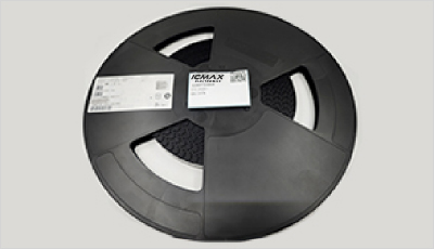
- Step1:Prepare product
-
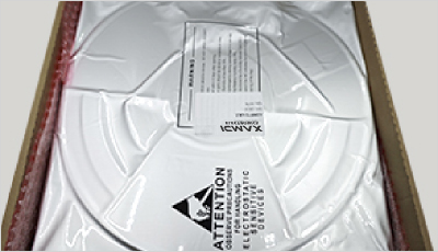
- Step2:Vacuum packaging
-
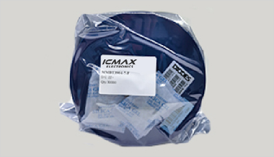
- Step3:Anti-static bag
-
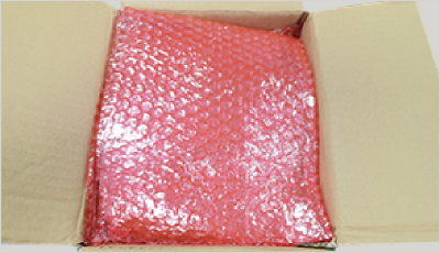
- Step4:Individual package
-
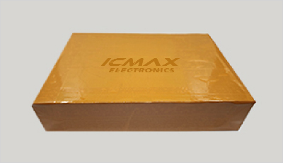
- Step5:Packaging box
-
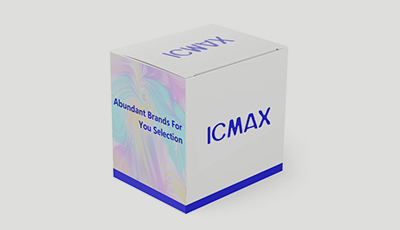
- Step6:Barcode shipping label
Shipping starts at $40, but some countries will exceed $40. For example (South Africa, Brazil, India, Pakistan, Israel, etc.)
The basic freight (for package ≤0.5kg or corresponding volume) depends on the time zone and country.
Currently, our products are shipped through DHL, FedEx, SF, and UPS.
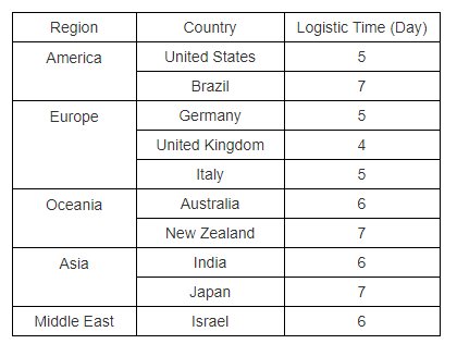
Delivery TimeOnce the goods are shipped, estimated delivery time depends on the shipping methods you chose:
FedEx International, 5-7 business days.
The following are some common countries' logistic time.
- Hot Sale
- Related Categories
- Include Parts
- Popular Search
The following parts include "MC74HC4052ADR2G" in Silicon Labs MC74HC4052ADR2G.
- Part Number
- Manufacturer
- Package
- Description
- SN74LVC1G3157DBVR Texas Instruments 16-SOIC (0.154", 3.90mm Width) IC SWITCH SP4T X 2 100OHM 16SOIC
- SN74LVC1G66DBVR Texas Instruments 16-SOIC (0.154", 3.90mm Width) IC SWITCH SP4T X 2 100OHM 16SOIC
- SN74LVC1G66DCKR Texas Instruments 16-SOIC (0.154", 3.90mm Width) IC SWITCH SP4T X 2 100OHM 16SOIC
- SN74LVC1G3157DSFR Texas Instruments 16-SOIC (0.154", 3.90mm Width) IC SWITCH SP4T X 2 100OHM 16SOIC
- 1P1G3157QDCKRQ1 Texas Instruments 16-SOIC (0.154", 3.90mm Width) IC SWITCH SP4T X 2 100OHM 16SOIC
- SN74LVC2G66DCUR Texas Instruments 16-SOIC (0.154", 3.90mm Width) IC SWITCH SP4T X 2 100OHM 16SOIC
- SN74LV4052APWR Texas Instruments 16-SOIC (0.154", 3.90mm Width) IC SWITCH SP4T X 2 100OHM 16SOIC
- 74HC4051D,653 Nexperia USA Inc. 16-SOIC (0.154", 3.90mm Width) IC SWITCH SP4T X 2 100OHM 16SOIC
- SN74LV4051APWR Texas Instruments 16-SOIC (0.154", 3.90mm Width) IC SWITCH SP4T X 2 100OHM 16SOIC
- CD74HC4052PWR Texas Instruments 16-SOIC (0.154", 3.90mm Width) IC SWITCH SP4T X 2 100OHM 16SOIC
The following parts are popular search parts in Test and Measurement.
Inventory:4,486
Please send an inquiry. Send us your inquiry, and we will respond immediately.

- 1500+ Daily average RFQ Volume

- 20,000.000 Standard Product Unit

- 1800+ Worldwide Manufacturers

- 15,000+ In-stock Warehouse


