


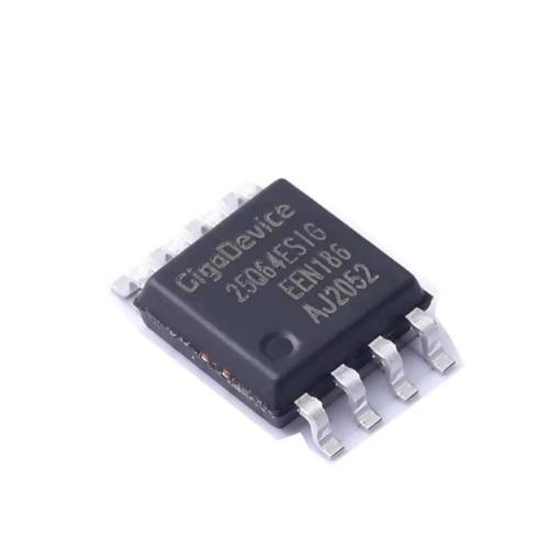
GigaDevice Semiconductor (HK) Limited GD25Q64ESIGR — 64Mbit SPI NOR Flash, 133MHz Quad I/O (SOP-8)

- Part No.:
- GD25Q64ESIGR — 64Mbit SPI NOR Flash, 133MHz Quad I/O (SOP-8)
- Manufacturer:
- GigaDevice Semiconductor (HK) Limited
- Category:
- Memory
- Package:
- 8-SOIC (0.209", 5.30mm Width)
 GD25Q64ESIGR — 64Mbit SPI NOR Flash, 133MHz Quad I/O (SOP-8).pdf
- Description:
- IC FLASH 64MBIT SPI/QUAD 8SOP
- Quantity:
-
Unit Price:$0
Ext Price:$0
- Payment:
-

- Shipping:
-


GD25Q64ESIGR — 64Mbit SPI NOR Flash, 133MHz Quad I/O (SOP-8) Information
- Specifications
- Product Details
- Comparison
- Tags
- Product attributes
- Attribute value
- Manufacturer:
- GigaDevice Semiconductor (HK) Limited
- Series:
- -
- Package/Case:
- 8-SOIC (0.209", 5.30mm Width)
- Packaging:
- Tape & Reel (TR)
- Product Status:
- Active
- Programmable:
- Not Verified
- Memory Type:
- Non-Volatile
- Memory Format:
- FLASH
- Technology:
- FLASH - NOR
- Memory Size:
- 64Mbit
- Memory Organization:
- 8M x 8
- Memory Interface:
- SPI - Quad I/O
- Clock Frequency:
- 133 MHz
- Write Cycle Time - Word, Page:
- 70µs, 2.4ms
- Access Time:
- 7 ns
- Voltage - Supply:
- 2.7V ~ 3.6V
- Operating Temperature:
- -40°C ~ 85°C (TA)
- Grade:
- -
- Qualification:
- -
- Mounting Type:
- Surface Mount
- Supplier Device Package:
- 8-SOP
GD25Q64ESIGR — 64Mbit SPI NOR Flash, 133MHz Quad I/O (SOP-8)
The GD25Q64ESIGR is a 64Mbit (8MB) SPI NOR Flash from GigaDevice, organised as 8M × 8-bit with a 133MHz maximum clock in Quad I/O mode. If you need non-volatile storage for firmware, calibration data, or a small file system, this part covers it in a single SOP-8 footprint.
It's the most common cross-reference swap for the Winbond W25Q64JV — same pinout, same voltage, same sector layout. But there's a catch engineers hit repeatedly: the QE (Quad Enable) bit defaults differently between the two parts. Firmware that assumes Quad mode is already on will read back garbage.
The fix is one status register write.
So why does this keep tripping people up? W25Q64 example code all over GitHub assumes QE is pre-set. The GD part looks identical on the scope until you switch to Quad mode.
If you know to look for it, you fix it in five minutes. If you don't, you spend an afternoon questioning your layout.
What Are the Technical Specifications of GD25Q64ESIGR?
| Parameter | Value |
|---|---|
| Memory Density | 64 Mbit (8 MB) |
| Memory Organization | 8M × 8-bit (uniform 4KB sectors / 64KB blocks) |
| Interface | SPI / Dual SPI / Quad SPI / QPI |
| Max Clock Frequency | 133 MHz (Quad I/O read) |
| Supply Voltage (VCC) | 2.7V – 3.6V |
| Active Read Current | 25 mA max @ 133 MHz |
| Standby Current | 40 µA max (12 µA typ) |
| Deep Power-Down Current | <5 µA typ |
| Page Program Time | 0.7 ms typ / 2.4 ms max |
| Sector Erase Time (4KB) | 45 ms typ / 100 ms max |
| Chip Erase Time | 20s typ / 40s max |
| Endurance | 100,000 Program/Erase cycles (minimum) |
| Data Retention | 20 years (minimum) |
| Package | SOP-8 208mil (5.28mm body width) |
| Operating Temperature | -40°C to +85°C |
| Manufacturer | GigaDevice Semiconductor |
The numbers that actually matter in a design review. The 100K P/E endurance matches Winbond's W25Q64JV — that's the industry baseline for this density, not a differentiator.
The standby current at 12µA typ means this flash won't kill your sleep budget in a battery-backed design. And the 0.7ms page program is fast enough that your MCU's SPI peripheral, not the flash, is the write bottleneck.
Throughput by SPI mode — same chip, very different real-world speeds. Quad I/O is the default choice for firmware XIP (execute-in-place). But if you're just storing a few config bytes, standard SPI at a relaxed clock is simpler to debug and less prone to signal integrity surprises on a 2-layer board.
Bar width = relative throughput at 133 MHz. Quad I/O gives 4× the throughput of standard SPI on the same clock. In practice, MCU SPI controller overhead and bus capacitance will knock 10–20% off these numbers.
SOP-8 pinout — standard 208mil footprint, identical to W25Q64JV. Pin 1 (CS#) is at the top-left with the dot marker. The pin mapping follows the industry-standard SPI NOR layout — if you've routed one of these before, you've routed them all.
Program and erase times vs the Winbond W25Q64JV. GD25Q64E is within 10–15% of Winbond on most operations. The gap is widest on chip erase, where GD takes about 5–7 seconds longer. For a production programmer that's noticeable; for a device that sees one firmware update in its lifetime, it's invisible.
Left bar = GD25Q64ESIGR typical; right bar (muted) = W25Q64JVSIQ typical. Both are within datasheet spec. No design change needed for the GD part unless your firmware has hard-coded timeout values calibrated to Winbond's timing.
When Should You Use (and NOT Use) the GD25Q64ESIGR?
✓ Use the GD25Q64ESIGR when:
- You're doing a W25Q64JV cost-down or second-source. Same footprint, same command set (with one caveat — see QE bit below). Drop it on the same PCB, update the JEDEC ID table in your bootloader, and test Quad mode entry.
- Your MCU has a QSPI peripheral and you want XIP (execute-in-place). At 133 MHz Quad I/O, the read throughput is enough to run most bare-metal firmware directly from flash without shadowing to RAM.
- You need industrial temperature range at a competitive price. -40°C to +85°C is standard on this part, no premium-tier suffix required.
- Power consumption matters. 12µA standby and sub-5µA deep power-down make it a fit for battery-powered data loggers and sensor nodes that wake, read, and sleep.
- You're building in China and want short lead times. GigaDevice parts move through Shenzhen distribution faster than most overseas NOR Flash brands.
✗ Don't use the GD25Q64ESIGR when:
- Your firmware uses QPI (Quad Peripheral Interface) mode and you can't modify the init sequence. The GD25Q64E enters QPI mode differently from the W25Q64JV. A firmware image compiled for Winbond QPI will not work without changes to the status register write sequence.
- You need 1.8V operation. This is a 3V part (2.7–3.6V). For 1.8V systems, use GD25LQ64ESIGR or W25Q64JW instead.
- Your boot ROM only recognizes Winbond JEDEC IDs and can't be updated. Some locked-down MCUs (certain STM32 boot ROMs, MediaTek router SoCs) have a fixed list of supported flash IDs. If GD isn't on the list, the chip won't boot — no workaround except changing the flash or the SoC.
- You're doing heavy data logging with frequent small writes and need the absolute fastest sector erase. GD's sector erase is ~45ms vs Winbond's ~40ms — negligible for most use cases, but it stacks up if you're erasing thousands of sectors per session.
What Are the Alternatives to GD25Q64ESIGR?
| Model | Manufacturer | Key Difference | Best For |
|---|---|---|---|
| W25Q64JVSSIQ | Winbond | Faster erase, wider ecosystem support | Drop-in replacement when firmware can't be changed |
| BY25Q64ASSIG | Boya | Domestic alternative, compatible command set | GD25Q64 cost-down, high-volume consumer |
| GD25Q64CSIG | GigaDevice | Same family, 120 MHz max (vs 133 MHz) | Lower-cost variant for ≤100 MHz designs |
| MX25L6433F | Macronix | Wider voltage range (1.65–3.6V on M2I-12G) | Mixed-voltage designs, automotive |
| W25Q64JWSSIQ | Winbond | 1.8V operation | Low-voltage systems |
| IS25LP064A | ISSI | Lower standby current, automotive qualified | Automotive & industrial with strict sleep budgets |
A common pattern: start with W25Q64JV for the first production run (fewer surprises), then add GD25Q64ESIGR as an approved second-source on the Rev 2 BOM. The two parts coexist on the same PCB with zero layout changes.
The only firmware delta is the JEDEC ID check and QE bit init. Maybe 10 lines of C.
What Are the Typical Applications of GD25Q64ESIGR?
MCU firmware storage. The dominant use case. GD25Q64ESIGR holds the bootloader, application code, and static assets (fonts, images, lookup tables). At 8MB, it fits a full FreeRTOS image plus a FAT filesystem with room to spare.
Most MCUs with a QSPI peripheral — STM32F4/F7/H7, ESP32, NXP i.MX RT, GigaDevice GD32 — can XIP directly from this flash.
IoT device configuration and OTA updates. The uniform 4KB sector size lets you erase and rewrite small blocks without touching adjacent sectors. An OTA update writes the new image to a secondary partition, verifies the CRC, flips a boot flag.
If power drops mid-update, the device isn't bricked. That's the whole point of A/B partitioning.
Router and networking equipment. GD25Q64-series parts are ubiquitous in consumer routers (Xiaomi, TP-Link, Tenda). The flash holds the bootloader (u-boot), the Linux kernel, and the root filesystem (SquashFS or JFFS2). If you repair routers, you'll see this chip more often than any other NOR Flash.
Data loggers and sensor nodes. The 12µA standby makes it viable for battery-powered devices that sample once per minute and log to flash. A 64Mbit density stores roughly 250,000 samples at 32 bytes each — months of data at typical sensor rates.
Gaming peripherals and HID firmware. Keyboards, mice, and game controllers store keymaps, lighting profiles, and macro sequences in SPI NOR Flash. At 8MB, GD25Q64ESIGR is overkill for a keyboard.
But here's the thing: it's often cheaper to buy the 64Mbit part in volume than a smaller-density chip from a slower-moving SKU. Economics beat engineering on this one.
GD25Q64ESIGR vs W25Q64JV: The Compatibility Reality
These two chips share the same footprint, the same voltage range, and roughly the same command set. But "pin-compatible" and "firmware-compatible" are not the same thing. So what actually breaks?
JEDEC Manufacturer ID. The GD25Q64E returns 0xC8 (GigaDevice); the W25Q64JV returns 0xEF (Winbond). If your bootloader has a whitelist of manufacturer IDs — and many do, especially on router SoCs — the system won't recognise the flash and will halt before reaching the kernel.
The fix is adding 0xC8 to the ID table. Two lines of code. But if the boot ROM is mask-programmed and you can't change it, this is a showstopper.
QE (Quad Enable) bit. This is the most common support issue on GD25Q64E. W25Q64JV often ships with the QE bit already set; GD25Q64ESIGR typically ships with QE=0. If your firmware tries a Quad I/O read without setting the QE bit first, the flash returns garbage.
Symptoms are easy to misdiagnose: the device boots fine, then hangs the moment it switches to Quad mode. Standard SPI reads work regardless of QE — that's why it gets past the bootloader.
The fix: a single Write Status Register command at init, setting S9 (QE) = 1. Make it the first SPI transaction after reading the JEDEC ID.
Status register layout. Writing Status Register 1 as a single byte — common in W25Q64 example code on GitHub — can silently clear Status Register 2 on the GD25Q64E. That wipes the QE bit you just set.
Always use the 16-bit Write Status Register command (0x01 with 2 data bytes) on this part. The 1-byte version happens to work on Winbond, so example code never catches it.
Why Buy GD25Q64ESIGR from ICMASS?
We stock the full GigaDevice GD25Q series. If you need GD25Q16, GD25Q32, GD25Q64, or GD25Q128 in any package variant (SOP-8, WSON, BGA), we carry them. One PO covers all your SPI Flash requirements.
Cross-reference support that goes beyond the datasheet. If you're migrating from W25Q64JV, MX25L6433F, or any other 64Mbit SPI NOR Flash, we'll walk you through the firmware changes: JEDEC ID, QE bit handling, status register layout differences. This is the stuff that burns your second day of bring-up.
Ships from Shenzhen. For prototype quantities (5–50 units), we ship within 24 hours. For production volumes, contact us for lead time and pricing on your specific quantity.
Frequently Asked Questions
Q1: Can I replace a W25Q64JV with a GD25Q64ESIGR without changing my PCB?
A: Yes, the hardware is 100% compatible. Same SOP-8 208mil footprint, same pinout, same voltage range. The PCB and solder stencil are identical. The firmware needs a JEDEC ID update and a QE bit initialisation routine — both are small changes, but they are mandatory, not optional.
Q2: Why does my device boot but then hang or corrupt data after switching to Quad SPI?
A: The QE (Quad Enable) bit is likely not set. Standard SPI reads (1-bit) work regardless of QE. The moment your firmware switches to Quad I/O read mode, the flash needs QE=1. If it's still 0, you get garbage data. Fix: issue a Write Status Register command (0x01, 2 bytes) with QE=1 during your flash init, right after reading the JEDEC ID.
Q3: Is the GD25Q64ESIGR slower than the W25Q64JV?
A: On paper, they're both 133 MHz. In practice, GD's program and erase times are 10–15% higher (e.g. sector erase 45ms vs 40ms). For a firmware storage application where you write once and read millions of times, this is invisible. For a data logger that erases and rewrites sectors continuously, it might add up. Most designs won't notice the difference.
Q4: Does GD25Q64ESIGR work with ESP32?
A: Yes, but use DIO (Dual I/O) mode, not QIO (Quad I/O). The ESP32 boot ROM is picky about flash QE bit handling. Flashing with --flash_mode dio is the safe default for GD25Q64E. If you need Quad I/O throughput, you can enable QIO in your application code after explicitly setting the QE bit — but don't rely on the boot ROM to do it for you.
Q5: What's the difference between GD25Q64ESIGR and GD25Q64CSIGR?
A: Clock speed and voltage tolerance. The 'E' version does 133 MHz at 2.7–3.6V. The 'C' version is rated for 120 MHz and some variants support a wider voltage range down to 1.65V. For most 3.3V designs, the 'E' version is the right pick. If your design runs at 1.8V, you need the 'L' series (GD25LQ64E), not either of these.
Q6: How do I check if my GD25Q64ESIGR is genuine?
A: Read the JEDEC ID (command 0x9F). A genuine GD25Q64E returns Manufacturer ID 0xC8, Memory Type 0x40, Capacity 0x17. If you get 0xEF (Winbond) or 0xC2 (Macronix) with GD25Q64 markings, the chip has been re-marked. Also check the QE bit default: most genuine GD25Q64E parts ship with QE=0. A "GD25Q64E" that shows up with QE=1 pre-set and a Winbond-style status register layout is suspicious.
Q7: Can I use GD25Q64ESIGR at 1.8V?
A: No. This is a 3V part (2.7–3.6V operating range). For 1.8V systems, use GD25LQ64ESIGR (GigaDevice's low-voltage series) or W25Q64JW (Winbond). Running a 3V flash at 1.8V will result in unreliable reads and writes, if it works at all.
Q8: What's the maximum SPI clock frequency I can reliably use?
A: 133 MHz per the datasheet, but your PCB layout sets the real limit. On a 2-layer board with long traces, back down to 80–100 MHz. Keep SPI traces short, route CLK with a ground return path, and avoid stubs. Community reports of instability above 26 MHz on some boards point to host PCB signal integrity, not a flash limitation. If your board is already laid out, start at 50 MHz and work up.
| Image |
|
| Part Number | GD25Q64ESIGR — 64Mbit SPI NOR Flash, 133MHz Quad I/O (SOP-8) |
| Manufacturer | GigaDevice Semiconductor (HK) Limited |
| Series | - |
| Package/Case | 8-SOIC (0.209", 5.30mm Width) |
| Packaging | Tape & Reel (TR) |
| Product Status | Active |
| Programmable | Not Verified |
| Memory Type | Non-Volatile |
| Memory Format | FLASH |
| Technology | FLASH - NOR |
| Memory Size | 64Mbit |
| Memory Organization | 8M x 8 |
| Memory Interface | SPI - Quad I/O |
| Clock Frequency | 133 MHz |
| Write Cycle Time - Word, Page | 70µs, 2.4ms |
| Access Time | 7 ns |
| Voltage - Supply | 2.7V ~ 3.6V |
| Operating Temperature | -40°C ~ 85°C (TA) |
| Grade | - |
| Qualification | - |
| Mounting Type | Surface Mount |
| Supplier Device Package | 8-SOP |
User Guide
- Purchase & Inquiry
- Package
- Shipping Information
- Customer Review
You may place an order without registering to IC-MAX.COM
We strongly suggest you sign in before purchasing as you can track your order in real time.
For your convenience, we accept multiple payment methods in USD, including PayPal, Credit Card, and wire transfer.
RFQ (Request for Quotations)
It is recommended to request for quotations to get the latest prices and inventories about the part.
Our sales will reply to your request by email within 24 hours.
1. You'll receive an order information email in your inbox. (Please remember to check the spam folder if you didn't hear from us).
2. Since inventories and prices may fluctuate to some extent, the sales manager is going to reconfirm the order and let you know if there are any updates.
-
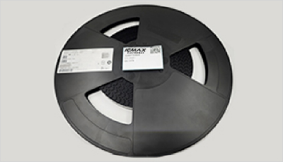
- Step1:Prepare product
-
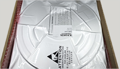
- Step2:Vacuum packaging
-
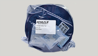
- Step3:Anti-static bag
-
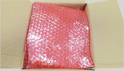
- Step4:Individual package
-
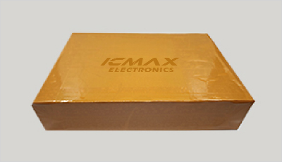
- Step5:Packaging box
-
- Step6:Barcode shipping label
Shipping starts at $40, but some countries will exceed $40. For example (South Africa, Brazil, India, Pakistan, Israel, etc.)
The basic freight (for package ≤0.5kg or corresponding volume) depends on the time zone and country.
Currently, our products are shipped through DHL, FedEx, SF, and UPS.
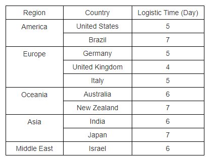
Delivery TimeOnce the goods are shipped, estimated delivery time depends on the shipping methods you chose:
FedEx International, 5-7 business days.
The following are some common countries' logistic time.
- Hot Sale
- Related Categories
- Include Parts
- Popular Search
The following parts include "GD25Q64ESIGR — 64Mbit SPI NOR Flash, 133MHz Quad I/O (SOP-8)" in Silicon Labs GD25Q64ESIGR — 64Mbit SPI NOR Flash, 133MHz Quad I/O (SOP-8).
- Part Number
- Manufacturer
- Package
- Description
- M24C02-WMN6TP STMicroelectronics 8-SOIC (0.209", 5.30mm Width) IC FLASH 64MBIT SPI/QUAD 8SOP
- AT24C02C-XHM-T Microchip Technology 8-SOIC (0.209", 5.30mm Width) IC FLASH 64MBIT SPI/QUAD 8SOP
- AT21CS01-STUM10-T Microchip Technology 8-SOIC (0.209", 5.30mm Width) IC FLASH 64MBIT SPI/QUAD 8SOP
- AT24C02C-SSHM-T Microchip Technology 8-SOIC (0.209", 5.30mm Width) IC FLASH 64MBIT SPI/QUAD 8SOP
- 24LC01BT-I/OT Microchip Technology 8-SOIC (0.209", 5.30mm Width) IC FLASH 64MBIT SPI/QUAD 8SOP
- M24C02-FMC6TG STMicroelectronics 8-SOIC (0.209", 5.30mm Width) IC FLASH 64MBIT SPI/QUAD 8SOP
- AT24CS02-SSHM-T Microchip Technology 8-SOIC (0.209", 5.30mm Width) IC FLASH 64MBIT SPI/QUAD 8SOP
- 93LC46BT-I/OT Microchip Technology 8-SOIC (0.209", 5.30mm Width) IC FLASH 64MBIT SPI/QUAD 8SOP
- AT24C04C-SSHM-T Microchip Technology 8-SOIC (0.209", 5.30mm Width) IC FLASH 64MBIT SPI/QUAD 8SOP
- 24LC01BT-I/SN Microchip Technology 8-SOIC (0.209", 5.30mm Width) IC FLASH 64MBIT SPI/QUAD 8SOP
The following parts are popular search parts in Test and Measurement.
Inventory:6,895
Please send an inquiry. Send us your inquiry, and we will respond immediately.

- 1500+ Daily average RFQ Volume

- 20,000.000 Standard Product Unit

- 1800+ Worldwide Manufacturers

- 15,000+ In-stock Warehouse


